
Design Guide

Platform Design Checklist
R
282 Intel
®
855GM/855GME Chipset Platform Design Guide
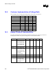
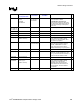
16.2. Customer Implementation of Voltage Rails
Fill in schematic name of voltage rails and mark boxes of when rails are powered on.
Name of Rail On S0-S1 On S3 On S4 On S5
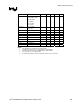
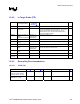
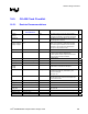
16.3. Design Checklist Implementation
The voltage rail designations in this Design Checklist are intended to be as general as possible. The
following table describes the equivalent voltage rails in the Intel CRB Schematics.
Checklist Rail Intel CRB Rail On S0-S1 On S3 On S4 On S5 Notes
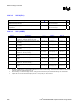
Vcc1_2
+V1.2S_GMCH_CORE,
+V1.2S_GMCH_HUB,
+V1.2S_GMCH_HGPLL,
+V1.2S_GMCH_DPLL,
+V1.2S_GMCH_ASM
X
Vcc1_25
+V1.25S [DDR_Vtt] X 4
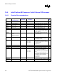
Vcc1_5 +V1.5S_GMCH_DVO,
+V1.5S_GMCH_ALVDS,
+V1.5S_GMCH_ADAC,
+V1.5S_GMCH_DLVDS,
+V1.5S_ICH,
+V1.5S_ICHHUB
X
VccSus1_5 +V1.5_ICHLAN X X 1,3
V1_5ALWAYS +V1.5A_ICH X X X X
VccSus2_5 +V2.5_GMCH_SM,
+V2.5_GMCH_QSM,
+V2.5_GMCH_TXLVDS,
+V2.5_DDR
X X