
Design Guide

Platform Design Checklist
R
Intel
®
855GM/855GME Chipset Platform Design Guide 283
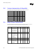
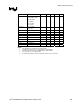
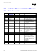
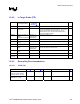
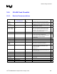
Checklist Rail Intel CRB Rail On S0-S1 On S3 On S4 On S5 Notes
Vcc3_3 +V3.3S_ICH,
+V3.3S_GMCH_GPIO,
+V3.3S_CLKRC,
+V3.3S_SPD,
+V3.3S_LVDS,
+V3.3S_FWH
X
VccSus3_3 +V3.3_ICHLAN,
+V3.3_LAN
X 1,2,3
V3ALWAYS +V3.3ALWAYS_ICH X X X X
Vcc5 +V5S_DAC X
VccSus5 +V5_USB X X 1,3
V5ALWAYS +V5A_ICH X X X X
Vcc12 +V12S X
VccRTC +V_RTC X X X X
VCCP
+VCC_IMVP X
VCCA +V1.8S_PROC X 5
VccCORE +VCC_CORE X
NOTES:
1. A rail powered in Sx is dependent on implementation.
2. VccLANx rail is powered on in Sx is dependent on implementation.
3. VxALWAYS rail can be the SUS rail depending on implementation.
4. Vcc1_25 is the 1.25 V VTT rail for DDR.
5. For Pentium M processor / Celeron M processor, VCCA is 1.8V, used for PLL.