
Design Guide

Platform Design Checklist
R
Intel
®
855GM/855GME Chipset Platform Design Guide 289
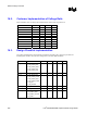
16.5. CK-408 Clock Checklist
16.5.1. Resistor Recommendations
Pin Name System
Pull-up/Pull-down
Series Resistor Notes
9
3V66[0]
3V66[1]
33
Ω
If the signal is used, one 33-ohm series resistor is
required. If the signal is NOT used, it should be left
as NC (Not Connected) or connected to a test point.
66BUF[2:0]
33
Ω
Use 66BUF[1] (pin 22) for GMCH. Use one of the
other two signals for ICH4-M.
CPU[0], CPU[0]#
CPU[1], CPU[1]#
CPU[2], CPU[2]#
49.9
Ω ± 1% pull- down to
gnd
33 Ω
Use one pair for the processor and another pair for
GMCH. If on-board ITP is implemented, the third
pair of clock signals is used for the ITP connector.
Otherwise, it can be routed to the dedicated ITP
clock pins on the processor socket.
48MDOT
33
Ω
Connect to GMCH’s DREFCLK.
3V66/VCH
33
Ω
Two possible topologies:
• Use directly for GMCH’s DREFSSCLK.
• Use as input to an SSC component and use the
SSC component output for GMCH’s
DREFSSCLK.
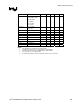
IREF
475
Ω ± 1% pull-down to gnd
MULT[0]
10 k
Ω pull-up to Vcc3_3
PCI[6:0]
33
Ω
Connect to various PCI devices.
PCIF[2],
PCIF[1],
PCIF[0]
33
Ω
Use one clock for ICH4-M. Unused clock pins should
be left as NC or connected to a test point.
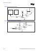
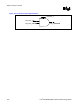
PWRDWN# AND gate This signal is needed for supporting S1M. It needs to
be driven low by both SLP_S1# and SLP_S3#
through an AND gate.
See Figure 151.
REF
33
Ω
This is the 14.318MHz clock reference signal for
ICH4-M, SIO and LPC. Each receiver requires one
33-ohm series resistor.
SEL[2:1]
10 k-20 k
Ω pull-down to gnd
SEL[0]
10 k-20 k
Ω pull- up to Vcc3_3
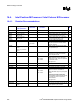
48MUSB
33
Ω
Connect to ICH4-M’s 48-MHz clock input.
XTAL_IN,
XTAL_OUT
Connect to a 14.318 MHz crystal, placed within 500
mils of CK-408
VDD[7:0], VDDA Connect to Vcc3_3 Refer to clock vendor datasheet for decoupling info.
VSS[5:0], VSSA Connect to gnd
VSSIREF Connect to gnd