
Design Guide

Platform Design Checklist
R
Intel
®
855GM/855GME Chipset Platform Design Guide 293
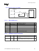
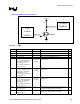
Figure 152. Reference Voltage Level for SMVREF
+
-
VccSus2_5
10k
+
/
-
1%
10k+/-1 %
SMVREF
GMCH
SMVREF_0
0.1 uF
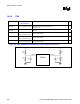
16.6.1.2. DDR SO-DIMM Interface
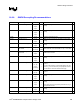
Pin Name Configuration Notes
9
VREF[2:1] Signal voltage level = VCCSus2_5 / 2.
VDD[33:1] Connect to VccSus2_5 Power must be provided during S3.
VDDSPD Connect to Vcc3_3
SA[2:0] Connect to either VC3_3 or
gnd
These lines are used for strapping the SPD address for each SO-DIMM.
VSS[31:1] Connect to gnd
RESET(DU) Signal can be left as NC (“Not Connected)
VDDID Signal can be left as NC (“Not Connected)
DU[4:1] Signal can be left as NC (“Not Connected)
GND[1:0] Signal can be left as NC (“Not Connected)
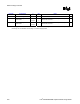
16.6.1.3. SODIMM Decoupling Recommendation
Pin Name F Qty Notes
9
Vcc1_25 0.1 µF
0.01 µF
Place one 0.1 µF cap and one 0.01 µF close to every 4 pull-up resistors
terminated to Vcc1_25 (VTT for DDR signal termination). In S3, Vcc1_25
is powered OFF.
Vcc2_5Sus 0.1 µF
100-150 µF
9
4
A minimum of 9 high frequency caps are recommeneded to be placed
bewteen the SO-DIMMS. A minimum of 4 low frequency caps are
required.