
Design Guide
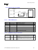

Platform Design Checklist
R
Intel
®
855GM/855GME Chipset Platform Design Guide 295
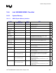
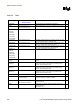
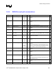
16.6.3. Hub Interface
Pin Name System
Pull-up/Pull-down
Notes
9
HLVREF See Section16.7.9. Signal voltage level = 0.35 V ± 8%.
PSWING See Section16.7.9. Signal voltage level = 2/3 of VCC1_2 or 0.8 V ± 8%.
HLZCOMP
27.4
Ω 1% pull-up to Vcc1_2
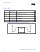
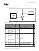
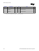
16.6.4. Graphics Interfaces
16.6.4.1. LVDS
Pin Name System
Pull-up/Pull-down
Notes
9
LIBG
1.5 K
Ω 1% pull-down to gnd
YAP[3:0]/YAM[3:0]
YBP[3:0]/YBM[3:0]
If any of these LVDS data pairs are unused, they can be left
as “no connect.”
CLKAP/CLKAM
CLKBP/CLKBM
If any of these LVDS clock pairs are not used, they can be left
as “no connect.”
LVREFH, LVREFL,
LVBG
These signals should be left as NC.