
Design Guide

Platform Design Checklist
R
Intel
®
855GM/855GME Chipset Platform Design Guide 297
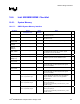
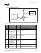
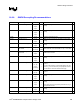
Figure 154. DPMS Clock Implementation
From
ICH4-M
SUSCLK
BSS138
3
1
2
1K
PM_SUS_CLK
Vcc1_5
SUS_CLK
To G MC H
DPMS pin
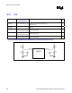
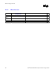
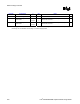
16.6.4.3. DAC
Pin Name System Pull-up /Pull-down In Series Notes
9
REFSET
127
Ω 1% pull-down to gnd
RED # Connect to gnd Need to connect to RED’s return path
BLUE # Connect to gnd Need to connect to BLUE’s return path
GREEN# Connect to gnd Need to connect to GREEN’s return path
RED On GMCH side of ferrite bead:
75
Ω 1% pull-down to gnd, 3.3
pF cap to gnd, ESD diode
protection for Vcc1_5
On VGA side of ferrite bead:
3.3 pF cap to gnd
Ferrite bead:
75
Ω at
100 MHz
Ferrite bead for EMI suppression between GMCH and
VGA connector.
BLUE On GMCH side of ferrite bead:
75
Ω 1% pull-down to gnd, 3.3
pF cap to gnd, ESD diode
protection for Vcc1_5
On VGA side of ferrite bead:
3.3 pF cap to gnd
Ferrite bead:
75
Ω at
100 MHz
Ferrite bead for EMI suppression between GMCH and
VGA connector.
GREEN On GMCH side of ferrite bead:
75
Ω 1% pull-down to gnd, 3.3
pF cap to gnd, ESD diode
protection for Vcc1_5
On VGA side of ferrite bead:
3.3 pF cap to gnd
Ferrite bead:
75
Ω at
100 MHz
Ferrite bead for EMI suppression between GMCH and
VGA connector.
HSYNC On VGA side of seires resistor:
33 pF cap to gnd
39
Ω
Use unidirectional buffer to prevent potential electrical
overstress and illegal operation of the GMCH.
VSYNC On VGA side of series resistor:
33 pF cap to gnd
39
Ω
Use to unidirectional buffer to prevent potential electrical
overstress and illegal operation of the GMCH.