
Design Guide

Platform Design Checklist
R
300 Intel
®
855GM/855GME Chipset Platform Design Guide
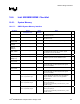
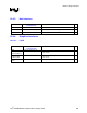
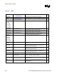
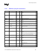
Pin Name Configuration F Qty Notes
9
VCCAGPLL Connect to Vcc1_2 0.1 µF 1
VCCADPLLA
Connect to Vcc1_2 with
network filter
0.1 µF
220 µF
1
1
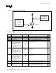
0.1 uH from power supply to GMCH pins, with caps on
GMCH side of inductor.
VCCADPLLB Connect to Vcc1_2 with
network filter
0.1 µF
220 µF
1
1
0.1 uH from power supply to GMCH pins, with caps on
GMCH side of inductor.
NOTE: Decoupling guidelines are recommendations based on our reference board design. Customers will need to take layout & PCB
board design into consideration when deciding on overall decoupling solution.