
Design Guide

Platform Design Checklist
R
Intel
®
855GM/855GME Chipset Platform Design Guide 303
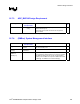
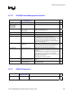
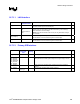
16.7.3. AGP_BUSY# Design Requirement
Signal System
Pull-up/Pull-down
Notes
9
AGPBUSY#
10 K
Ω pull-up to
Vcc3_3
This ICH4-M signal requires a pull-up to the switched 3.3-V rail
(powered OFF during S3).
This ICH4-M signal must be connected to the AGP_BUSY#
output of GMCH.
NOTE: Please also consult Intel for the latest AGP Busy and Stop signal implementation.
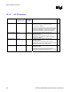
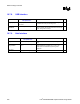
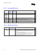
16.7.4. (SMBus) System Management Interface
Pin Name System
Pull-up/Pull-down
Notes
9
SM_INTRUDER#
100 k
Ω pull-up to
VccRTC
RTC well input requires pull-up (10 k-100 k) to reduce leakage
from coin cell battery in G3.
SMB_ALERT#/
GPIO[11]
10 k
Ω pull-up to
V3ALWAYS
SMBCLK,
SMBDATA,
SMLINK[1:0]
Pull-up to V3ALWAYS Require external pull-up resistors. Pull up value is determined by
bus characteristics. CRB schematics use 10 k
Ω pull-up resistors.
The SMBus and SMLink signals must be connected together
externally in S0 for SMBus 2.0 compliance: SMBCLK connected
to SMLink[0] and SMBDATA connected to SMLink[1].