
Design Guide

Platform Design Checklist
R
306 Intel
®
855GM/855GME Chipset Platform Design Guide
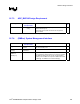
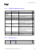
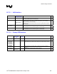
16.7.8. USB Interface
Pin Name System
Pull-up/Pull-down
Notes
9
USB_OC[5:0]#
10 k
Ω pull-up to V3ALWAYS
if not driven
No pull-up is required if signalsl are driven.. Signals
must NOT float if they are not being used.
USBRBIAS,
USBRBIAS#
22.6
Ω ± 1% pull-down to gnd
Connect signals together and pull down through a
common resistor, placed within 500 mils of the ICH4-M.
Avoid routing next to clock pin.
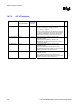
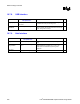
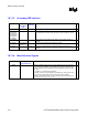
16.7.9. Hub Interface
Pin Name System
Pull-up/Pull-down
Notes
9
HUB_RCOMP
48.7
Ω 1% pull-up to to Vcc1_5
Place resistor within 0.5” of ICH4-M pad using a thick
trace.
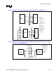
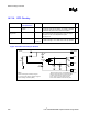
HUB_VREF,
HUB_VSWING
See Figure 155 and Figure
156.
HUB_VREF signal voltage level = 0.35 V ± 8%.
HUB_VSWING signal voltage level = 0.80 V ± 8%.
Three options are available for generating these
references.
HUB_PD11
56
Ω pull-down to gnd