
Design Guide

Platform Design Checklist
R
308 Intel
®
855GM/855GME Chipset Platform Design Guide
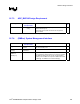
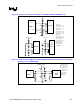
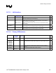
16.7.10. RTC Circuitry
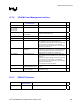
Pin Name System
Pull-up/Pull-down
In Series Notes
9
RTCRST#
180 k
Ω pull-up to
VccRTC
RTCRST# requires 18-25 ms delay. Use a 0.1 µF cap to
ground Pull up with 180 k
Ω resistor. Any resistor or capacitor
combination that yields a time constant is acceptable.
CLK_RTCX1,
CLK_RTCX2
Connect a 32.768 kHZ crystal oscillator across these pins
with a 10 M
Ω resistor and a decoupling cap at each signal.
Values for C1 and C2 are dependent on crystal.
See Figure 157.
CLK_VBIAS
1 K
Ω
0.047 µF
Connect to CLK_RTCX1 through a 10 MΩ resistor. Connect
to VBATT through a 1 k
Ω in series with a 0.047 µF capacitor.
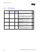
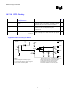
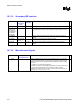
Figure 157. External Circuitry for the RTC
32.768 kHz
Xtal
0.047uF
10M
Ω
VCCRTC
RTCX2
RTCX1
VBIAS
Vbatt
1uF
1k
Ω
3.3V Sus
10M
Ω
C1 C2
C3
R1
R2
Notes
Reference Designators Arbitrarily Assigned
3.3V Sus is Active Whenever System Plugged In
Vbatt is Voltage Provided By Battery
VBIAS, VCCRTC, RTCX1, and RTCX2 are ICH4-M pins
VBIAS is used to bias the ICH4 Internal Oscillator
VCCRTC powers the RTC well of the ICH4-M
RTCX1 is the Input to the Internal Oscillator
RTCX2 is the feedback for the external crystal