
Design Guide


A
A
B
B
C
C
D
D
E
E
4 4
3 3
2 2
1 1
PG 24
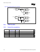
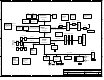
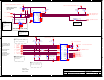
855GM/GME
GMCH
PG 23
PG 37
(Docking)
ICH4-M
USB 2.0
ADD Card
Connector
421 BGA
PG 28
DDR SDRAM
Intel 855GM: 200/266 MHz
Intel 855GME: 200/266/333 MHz
CPU
Thermal
Sensor
1.5V Always,
5V Always
1.5V
DVO Bus
PG 37
PG 35
SODIMM1
PG 5
478 uFCPGA
PG 36
PG 38
PORT 80--83
5V PCI SLOT 1
LPC
SLOT
Clocking
732 uFCBGA
33MHz PCI
Docking
Connector
PG 7,8,9,10
5V PCI SLOT 2
PG 14
DAC
RJ45
PG 27
USB2
PG 25
PG 39,40,41
Turner
System
DC/DC
Connector
MDC
Header
8 Mbit
PG 26,27
PG 30
Scan
KB
Hub Interface
66MHz
PG 36
CK-408
PG 45
(CRT) PG 17
PG 32
855GME VR
LVDS
PG 29
USB1
PG 13
SODIMM0
USB4
PG 35
PG 29
PG 28
PS/2
PG 37
PG 16
PG 43
PG 6
PG 46
PG 34
IMVP-IV VR
IDE0
PG 33
PG 35
IDE1
PG 12
Q-Switch
Backlight
Connector
SMC/KBC
LPC PM
Headers
Fan
Header
Test Points
Serial
AC97
PG 35
DDR VR
5V PCI SLOT 3
82562EM
PG 36
PG 15
Processor
FDD
SIO
PG 13
FIR
PG 33
PG 10
USB5
USB0
On Board VR
PG 21
Hitachi H8S
2149
ITP
PG 31
PG 16
PG 22
PG 28
PG 5
USB3
EVMC SLOT
SS
Clocking
PG 11
PG 44
Suspend
Timer
PG 6
PG 22
PG 3,4
Parallel
LAN CONNECT
PS/2
LPC, 33MHz
ATA 100
FWH
PG 29
PSB
PG 18,19,20,21
PC87393
4.401
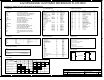
BLOCK DIAGRAM
A
150Monday, September 15, 2003
Intel 855GM/GME CRB
Title
Size Document Number Rev
Date: Sheet
of
Project: