
Design Guide

A
A
B
B
C
C
D
D
E
E
4 4
3 3
2 2
1 1
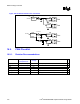
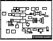
SCHEMATIC ANNOTATIONS AND BOARD INFORMATION
Intel 855GM/GME CUSTOMER REFERENCE PLATFORM
SMB_ICH
56
LOW
Device
Suffix
ON
I1-I4
Full ON
Smart Battery
SMB_ICH
1001 000x
2
HIGH
SMB_ICH
ReferencePC/PCI
51
OFF
Power States
SW8A1
3
Slot 3
16
__
LOW
ON
90
27
SMB_ICH
Device
SOT23-5
SMB_ICH
54
0101 0100
SMB_SB
45
OFF
5
SMC/KBC Caps Lock
____ ____
SMB_ICH
SMB_ICH
14
SMB_ICHPV4
VID0
Page
__
Clocks
SMC/KBC Num Lock
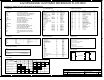
I C / SMB Addresses
SIGNAL
57
SMB_ICH_S
38
Bluetooth Header
Reference
A2
LOW
34
SMB_ICH
OFFLOW
Virtual Battery On/Off
59
____ ____
LOW
3
SOT-23
53
____ ____
+V*S
LOW
DS2J2
Switch
D2
Smart Selector
LED
32
38
V1-V4
34
1001 110x
SW7J1
Address
SLP_S3#
52
Slot 2
LPC Pwr Mngmnt Header __
A0
As seen from top
58
A
HIGH
38
0101 1001
Voltage Rails
45
SMC/KBC Scroll Lock
OFF
SLP_S1#
34
9C
SMB_SB
HIGH
2
OFF
SMB_SB
DS1J3
SMB_THRM
SMB_SB
1
SMB_ICH
Prefix
SLP_S4#
1101 001x
A
DS1H1
0101 0010
LOW
ON
34
SMB_THRM
Page
PCB Footprints
HIGH
0001 011x
DS1J4
__
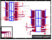
SO-DIMM1
Secondary IDE
Thermal Diode
27
+VDC
+VCC_CORE
+VCCP
+V1.8S
+V1.25S
+V1.35S
+V1.5S
+V1.5ALWAYS
+V1.5
+V2.5
+V3.3ALWAYS
+V3.3
+V3.3S
+V5ALWAYS
+V5
+V5S
+V12S
-V12S
HIGH
DS1J1LAN
0001 010x
SMB_ICH_S
DS1H3
VID1
V5-V8
DS1J2
LPC Pwr Mngmnt Header
Primary DC system power supply (10 to 21V)
Core voltage for processor
1.05V rail for processor PSB, 855GME PSB
1.8V for processor PLL and VID circuitry
1.25V DDR Termination voltage
1.35V for 855GM core
1.5V switched power rail (off in S3-S5)
1.5V always on power rail
1.5V power rail (off in S4-S5)
2.5V power rail for DDR
3.3V always on power rail
3.3V power rail (off in S4-S5)
3.3V switched power rail (off in S3-S5)
5.0V for ICH4M's VCC5REFSUS
5.0V power rail (off in S4-S5)
5.0V switched power rail (off in S3-S5)
12.0V switched power rail (off in S3-S5)
-12.0V switched power rail for PCI (off in
S3-S5)
DS2J3
____ ____
OFF
Reset
DS8B1
SMB_ICHLVDS Backlight Inverter
+V*
LOW
VID2
Bus
Primary IDE
1
32
LOW
S3 State
S0 State
EV Support:
0101 0011
S4 (Suspend To Disk)
32
Lid
Dock Connector
____ ____
A
1010 001x
DS1H2
VID3
+V*ALWAYS
ON
SMB_ICH_S
S1M (Power On Suspend)
STATE
Wake Events
S4 State
S1 State
OFF
DS2J1
PV0-PV3
SMB_ICH
__
DS2H2
VID4
LEDs and Switches
ON
ON
32
SMB_SB
S5 State
0101 0001
0101 0100
SW9A1
LOW
DS2H1
34
12
0101 0101
0001 001x
HIGH
Slot 1
38
DV0-DV3
Smart Battery Charger
B
HIGH
DV4
HIGH
DS8A2
SW8J1
ON
SLP_S5#
1010 000x
V9-V12
Clock Generator
OFF
ONHIGH
SO-DIMM0
38
0101 0111
SMB_ICH_S
ON
Net Naming Conventions
55
Power On/Off
ON
S3 (Suspend to RAM)
S5 / Soft OFF
32
0101 0110
2
Hex
DS8A1
LOW
EP1-EP4
Thermal Sensor Header
Spread Spectrum Clock
HIGH
4
ON
TP = Test Point (does not
connect anywhere else)
Default DescriptionJumper PageOption
D41101 010x
VID5 34 DS2J4
H = Host
M = DDR Memory
# = Active Low Signal
RI# (Ring Indicate) from serial port
PME# (Power Management Event) from PCI/mini-PCI slots,
ADD slot, LPC slot
LAN Connect Interface from 82562EM
LID switch attached to SMC
USB
AC97 wake on ring
SmLink for AOL II
Hot Key from the scan matrix keyboard
REQ/GNT #
4 B, C, D, A
AD18
(E, F, G, H optional)
IDSEL #
PCI Devices
C, D, B, A
G, F, E, H
AD16
3
(AD24 internal)
4
2
Interrupts
AD28
A, B
F, G, H, E1
Docking
3
1
AD17 2
Default Jumper Settings
J4F1 1-X 09No-Shunt Default1-2
CMOS Clear
J9H1
19
J9A1
Moon ISA Support
2-3
2-3
1-2
19
33
1-2
Moon ISA Support
23
34
2-3
SIO Disable
1-2
SMC/KBC ProgrammingJ9B1
1-2
J8A1
J9A3 SMC_LID Disable 321-X 1-2
1-X 1-2
1-X 1-2
1-X
1-2
1-X
1-X
1-X
1-X
LVDS EV
GMCH Strap: Clock Config
J3G1
1-2
08
J7B5
1-2 DDR EV Support
GMCH Strap: PSB Voltage
08
44
08
2-3
1-2
GMCH Strap: Clock Config
J7B2
1-2
1-2
GMCH Strap: Clock Config
081-X
1-2
J7B4
J7B3
No-Shunt Default1-2J6D1 1-X 09
1-X
1-2 23
1-X
32
SMC/KBC Disable
32
2-3
33
J9E4
1-2
J9E5
1-2
1-2
J8J2
J2J3
J9E2 23
1-X
J9G2
2-3
Port 80-81/82-83 Select
J8A2 32
1-2
2-3
Moon ISA Support
1-2
NMI Jumper
1-X
CRB/SV Detect
KBC 60/64 Decode Disable
J1H5
J1H4 46
46
A_FAN_P1
A_FAN_P0
GMCH Strap: DVO Strap
08
J6E1
1-2
J7C1
08
1-X
4.401
Notes and Annotations
A
250Monday, September 15, 2003
Intel 855GM/GME CRB <Doc>
Title
Size Document Number Rev
Date: Sheet
of
Project: