
Design Guide


General Design Considerations
R
Intel
®
855GM/855GME Chipset Platform Design Guide 33
3. General Design Considerations
This section documents motherboard layout and routing guidelines for the Intel 855GM/GME chipset
based systems. It does not discuss the functional aspects of any bus, or the layout guidelines for an add-
in device.
If the guidelines listed in this document are not followed, it is important that thorough signal integrity
and timing simulations are completed for each design. Even when the guidelines are followed, Intel
recommends that critical signals be simulated to ensure proper signal integrity and flight time. Any
deviation from the guidelines should be simulated.
The trace impedance typically noted (i.e. 55 Ω ± 15%) is the “nominal” trace impedance for a 5-mil
wide external trace and a 4-mil wide internal trace. However, some stack-ups may lead to narrower or
wider traces on internal or external layers in order to meet the 55-Ω impedance target, that is, the
impedance of the trace when not subjected to the fields created by changing current in neighboring
traces. Note the trace impedance target assumes that the trace is not subjected to the EM fields created
by changing current in neighboring traces. It is important to consider the minimum and maximum
impedance of a trace based on the switching of neighboring traces when calculating flight times. Using
wider spaces between the traces can minimize this trace-to-trace coupling. In addition, these wider
spaces reduce settling time.
Coupling between two traces is a function of the coupled length, the distance separating the traces, the
signal edge rate, and the degree of mutual capacitance and inductance. In order to minimize the effects
of trace-to-trace coupling, the routing guidelines documented in this Section should be followed. Also,
all high speed, impedance controlled signals should have continuous GND referenced planes and cannot
be routed over or under power/GND plane splits.
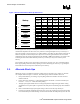
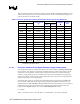
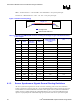
3.1. Nominal Board Stack-Up
The Intel 855GM/GME chipset based platforms require a board stack-up yielding a target impedance of
55 Ω ± 15%. An example of an 8-layer board stack-up is shown in Figure 3. The left side of the figure
illustrates the starting dimensions of the metal and dielectric material thickness as well as drawn trace
width dimensions prior to lamination, conductor plating, and etching. After the motherboard materials
are laminated, conductors plated, and etched, somewhat different dimensions will result. Dielectric
materials become thinner, under/over etching of conductors alters their trace width, and conductor
plating makes them thicker. It is important to note that for the purpose of extracting electrical models
from transmission line properties, the final dimensions of signals after lamination, plating, and etching
should be used.
The stack-up uses 1.2-mil (1 oz) copper on power planes to reduce I*R drops and 0.6-mil copper
thickness on the signal layers: primary side layer (L1), Layer 3 (L3), Layer 6 (L6), and secondary side
layer (L8). After plating, the external layers become 1.2 to 2 mils thick.
To ensure impedance control of 55 Ω, the primary and secondary side layer micro-strip lines should
reference solid ground planes on Layer 2 and Layer 7, respectively.