
Design Guide


General Design Considerations
R
34 Intel
®
855GM/855GME Chipset Platform Design Guide
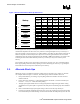
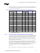
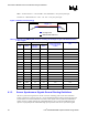
Figure 3. Recommended Board Stack-Up Dimensions
Dielectric Layer Layer Copper Trace Trace
Thickness No. Type
Weight Width Impedance
S
1 SIGNAL 1/2+plating
5.0 55
=> 5.0
P2PLANE1
=> 5.0
S
3SIGNAL1
4.0 55
=> 12.0
P
4PLANE1
=> 10.0
P
5PLANE1
=> 12.0
S
6SIGNAL1
4.0 5
5
=> 5.0
P
7PLANE1
=> 5.0
8 SIGNAL 1/2+plating
5.0 5
5
S
PREPREG
CORE
PREPREG
CORE
PREPREG
PREPREG
CORE
(mils) (ohms)
Stackup
(oz)(mils)
Internal signal traces on Layer 3 and Layer 6 are unbalanced strip-lines. To meet the nominal 55-Ω
characteristic impedance for these traces, they reference a solid ground plane on Layer 2 and Layer 7.
Since the coupling to Layer 4 and Layer 5 is still significant, (especially true when thinner stack-ups use
balanced strip-lines on internal layers) these layers are converted to ground floods in the areas of the
motherboard where the speed critical interfaces like the PSB or DDR system memory are routed. In the
remaining Sections of the motherboard layout the Layer 4 and Layer 5 layers are used for power
delivery.
The secondary side layer (L8) is also used for power delivery in many cases, since it benefits from the
thick copper plating of the external layer plating as well as referencing the close Layer 7 ground plane.
The benefit of such a stack-up is low inductance power delivery.
3.2. Alternate Stack Ups
OEMs may choose to use different stack-ups (number of layers, thickness, trace width, etc.) from the
one example outlined in Figure 3. However, the following key elements should be observed:
1. Final post lamination, post etching, and post plating dimensions should be used for electrical
model extractions.
2. Power plane layers should be 1 oz thick and signal layers should be ½ oz thick. External layers
become 1 – 1.5 oz (1.2 – 2 mils) thick after plating.
3. All high-speed signals should reference solid ground planes through the length of their routing
and should not cross plane splits. To guarantee this, both planes surrounding strip-lines should be
GND.
4. Intel recommends that high-speed signal routing be done on internal, strip-line layers.
5. For high-speed signals transitioning between layers next to the component, the signal pins should
be accounted for by the GND stitching vias that would stitch all the GND plane layers in that area