
Design Guide


Intel Pentium M/Celeron M Front Side Bus Design Guidelines
R
Intel
®
855GM/855GME Chipset Platform Design Guide 37
4. Intel Pentium M/Celeron M Front
Side Bus Design Guidelines
The following layout guidelines support designs using the Intel Pentium M processor or Intel Celeron
processor and the Intel 855GM/GME GMCH chipset. Due to on-die Rtt resistors on both the processor
and the chipset, additional resistors do not need to be placed on the motherboard for most PSB signals.
A simple point-to-point interconnect topology is used in these cases.
4.1. Intel Pentium M Processor / Intel Celeron M FSB
Design Recommendations
For proper operation of the Intel Pentium M / Intel Celeron M processor and the GMCH PSB interface,
it is necessary that the system designer meet the timing and voltage specification of each component.
The following recommendations are Intel’s best guidelines based on extensive simulation and
experimentation that make assumptions, which may be different than an OEM’s system design. The
most accurate way to understand the signal integrity and timing of the FSB in your platform is by
performing a comprehensive simulation analysis. It is possible that adjustments to trace impedance, line
length, termination impedance, board stack-up, and other parameters can be made that improve system
performance.
Refer to the latest Intel
®
Pentium
®
M Processor Datasheet or Intel Celeron M Datasheet for a FSB
signal list, signal types, and definitions. Below are the design recommendations for the data, address,
and strobes. For the following discussion, the pad is defined as the attach point of the silicon die to the
package substrate. The following topology and layout guidelines are preliminary and subject to change.
The guidelines are derived from empirical testing with GMCH package models.
4.1.1. Recommended Stack-up Routing and Spacing Assumptions
The following section describes in more detail, the terminology and definitions used for different routing
and stack-up assumptions that apply to the recommended motherboard stack-up show in Section 3.1.
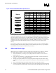
4.1.1.1. Trace Space to Trace – Reference Plane Separation Ratio
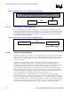
Figure 4 illustrates the recommended relationship between the edge-to-edge trace spacing (2X) versus
the trace to reference plane separation (X). An edge-to-edge trace spacing (2X) to trace – reference
plane separation (X) ratio of 2 to 1 ensures a low crosstalk coefficient. All the effects of crosstalk are
difficult to simulate. The timing and layout guidelines for the processor have been created with the
assumption of a 2:1 trace spacing to reference plane ratio. A smaller ratio would have an unpredictable
impact due to crosstalk.