
Design Guide


Intel Pentium M/Celeron M Front Side Bus Design Guidelines
R
Intel
®
855GM/855GME Chipset Platform Design Guide 39
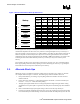
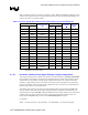
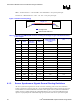
Table 2 summarizes the list of common clock and key routing. RESET# (CPURST# of GMCH) is also a
common clock signal but requires a special treatment for the case where an ITP700FLEX debug port is
used. See Section 4.1.5 for further details.
Table 2. Processor System Bus Common Clock Signal Internal Layer Routing Guidelines
Signal Names Total Trace Length
CPU GMCH
Transmission Line
Type
Min
(mils)
Max
(inches)
Nominal
Impedance
(
Ω)
Spacing &
Width
ADS# ADS# Strip-line 997 6.5 55 ± 15% 2:1
BNR# BNR# Strip-line 1298 6.5 55 ± 15% 2:1
BPRI# BPRI# Strip-line 1215 6.5 55 ± 15% 2:1
BR0# BR0# Strip-line 1411 6.5 55 ± 15% 2:1
DBSY# DBSY# Strip-line 1159 6.5 55 ± 15% 2:1
DEFER# DEFER# Strip-line 1291 6.5 55 ± 15% 2:1
DPWR# DPWR# Strip-line 1188 6.5 55 ± 15% 2:1
DRDY# DRDY# Strip-line 1336 6.5 55 ± 15% 2:1
HIT# HIT# Strip-line 1303 6.5 55 ± 15% 2:1
HITM# HITM# Strip-line 1203 6.5 55 ± 15% 2:1
LOCK# HLOCK# Strip-line 1198 6.5 55 ± 15% 2:1
RS0# RS0# Strip-line 1315 6.5 55 ± 15% 2:1
RS1# RS1# Strip-line 1193 6.5 55 ± 15% 2:1
RS2# RS2# Strip-line 1247 6.5 55 ± 15% 2:1
TRDY# HTRDY# Strip-line 1312 6.5 55 ± 15% 2:1
RESET#
1
CPURST# Strip-line 1101 6.5 55 ± 15% 2:1
NOTE: For topologies where an ITP700FLEX debug port is implemented, see Section 4.1.5 for RESET#
(CPURST#) implementation details.
4.1.2.1. Processor Common Clock Signal Package Length Compensation
Trace length matching for the common clock signals is not required. However, package compensation
for the common clock signals is required for the minimum board trace. Please refer to Table 3 and the
example below for more details. Package length compensation should not be confused with length
matching. Length matching refers to constraints on the min and max length bounds of a signal group
based on clock length, whereas package length compensation refers to the process of compensating for
package length variance across a signal group.
All common clock signals are required to meet the minimum pad-to-pad requirement of 2.212 inches,
based on ADS# (as this signal has the longest package lengths). This implies a minimum pin-to-pin
motherboard trace length of 997 mils. Additional motherboard trace will be added to some of the shorter
common clock nets on the system board in order to meet the same minimum requirement for trace
lengths from the die-pad of the processor to the associated die-pad of the chipset.
For example:
ADS# = 997 mils board trace + 454 CPU PKG + 761 GMCH PKG = 2212 pad-to-pad length