
Design Guide


Intel Pentium M/Celeron M Front Side Bus Design Guidelines
R
40 Intel
®
855GM/855GME Chipset Platform Design Guide
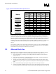
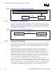
BR0# = X mils board trace + 336 CPU PKG + 465 GMCH PKG = 2212 pad-to-pad length
Therefore: X = BR0# board trace = 2212 - 336 - 465 = 1411 pin to pin length.
Figure 6. Common Clock Topology
GMCH
Processor
Length L1
Package trace
Motherboard PCB trace
Pad
Pad
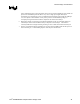
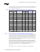
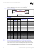
Table 3. Processor and GMCH PSB Common Clock Signal Package Lengths and Minimum Board
Trace Lengths
Signal Names Package Length
CPU GMCH
Intel Pentium
M/Celeron
Processor
GMCH
Total Pad-to-Pad Min.
Length Requirements
L1 (mils)
Min. Board Trace Length
(mils)
ADS# ADS# 454 761 2212 997
BNR# BNR# 506 408 2212 1298
BPRI# BPRI# 424 573 2212 1215
BR0# BR0# 336 465 2212 1411
DBSY# DBSY# 445 608 2212 1159
DEFER# DEFER# 349 572 2212 1291
DPWR# DPWR# 506 518 2212 1188
DRDY# DRDY# 529 347 2212 1336
HIT# HIT# 420 489 2212 1303
HITM# HITM# 368 641 2212 1203
LOCK# HLOCK# 499 515 2212 1198
RS0# RS0# 576 321 2212 1315
RS1# RS1# 524 495 2212 1193
RS2# RS2# 451 514 2212 1247
TRDY# HTRDY# 389 511 2212 1312
RESET# CPURST# 455 656 2212 1101
4.1.3. Source Synchronous Signals General Routing Guidelines
All source synchronous signals use an AGTL+ bus driver technology with on-die GTL termination
resistors connected in a point-to-point, Zo = 55 Ω controlled impedance topology between the processor
and the GMCH. No external termination is needed on these signals. Source synchronous PSB address
signals operate at a double pumped rate of 200 MHz while the source synchronous PSB data signals
operate at a quad pumped rate of 400 MHz. High-speed operation of the source synchronous signals