
Design Guide

Intel Pentium M/Celeron M Front Side Bus Design Guidelines
R
Intel
®
855GM/855GME Chipset Platform Design Guide 41
requires careful attention to their routing considerations. The following guidelines should be strictly
adhered to, to guarantee robust high frequency operation of these signals.
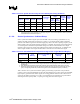
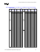
Source synchronous data and address signals and their associated strobes are partitioned into groups of
signals. Flight time skew minimization within the same group of source synchronous signals is a key
parameter that allows their high frequency (400 MHz) operation. All the source synchronous signals that
belong to the same group should be routed on the same internal layer for the entire length of the bus.
It is OK to split different groups of source synchronous signals between different motherboard layers as
long as all the signals that belong to that group are kept on the same layer. Grouping of PSB source
synchronous signals is summarized in Table 4 and Table 6. This practice results in a significant
reduction of the flight time skew since the dielectric thickness, line width, and velocity of the signals
will be uniform across a single layer of the stack-up.
The source synchronous signals should be routed as a strip-line on an internal layer with complete
reference to ground planes both above and below the signal layer. Routing with references to split
planes or power planes other than ground is not recommended. For the recommended stack-up example
as shown in Figure 3, source synchronous PSB signals are routed on Layer 3 and Layer 6. Layer 2 and
Layer 7 are solid grounds across the entire motherboard. However, this is not sufficient since significant
coupling exists between signal layer, Layer 3 and power plane Layer 2 as well as signal layer, Layer 6
and power plane Layer 5. To guarantee complete ground referencing, Layer 4 and Layer 5 are converted
to ground plane floods in the areas where the source synchronous PSB signals are routed. In addition all
the ground plane areas are stitched with ground vias in the vicinity of the processor and the GMCH
package outlines with the vias of the ground pins of the processor and the GMCH pin-map.
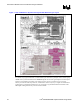
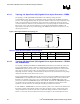
Figure 7 illustrates a motherboard layout of the recommended stack-up of the PSB source synchronous
DATA and ADDRESS signals referencing ground planes on both Layer 7 and Layer 5. Note that in the
socket cavity of the processor, Layer 5 and Layer 6 is used for VCC core power delivery. However,
outside the socket cavity Layer 6 signals are routed on top of a solid Layer 7 ground plane and also
Layer 5 is converted to a ground flood under the shadow of the PSB signals routing between the
processor and the GMCH. Stitching of all the GND planes is provided by the ground vias in the pin-map
of the processor and the GMCH.