
Design Guide

Intel Pentium M/Celeron M Front Side Bus Design Guidelines
R
42 Intel
®
855GM/855GME Chipset Platform Design Guide
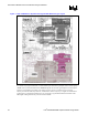
Figure 7. Layer 6 PSB Source Synchronous Signals GND Referencing to Layer 5
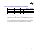
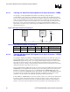
In a similar way, Figure 8 illustrates a recommended layout and stack-up example of how another group
of PSB source synchronous DATA and ADDRESS signals can reference ground planes on both Layer 2
and Layer 4. Note that in the socket cavity of the processor, Layer 3 is used for VCC core power
delivery to reduce the I*R drop. However, outside of the socket cavity Layer 3 signals are routed below
a solid Layer 2 ground plane and also Layer 4 is converted to a ground flood under the shadow of the
PSB signals routing between the processor and the GMCH.