
Design Guide

Intel Pentium M/Celeron M Front Side Bus Design Guidelines
R
52 Intel
®
855GM/855GME Chipset Platform Design Guide
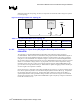
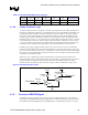
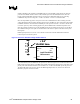
Figure 11. Routing Illustration for Topology 1C
CPU
L1
L3
L2
Rs
3.3
3904
3904
L4
3.3
Q1
Q2
R1
R2
V_IO_RCVR
(System receiver)
VCCP
Rtt
Table 12. Layout Recommendations for Topology 1C
L1 L2 L3 L4 Rs R1 R2- Rtt Transmission
0.5” – 12.0” 0” – 3.0” 0” – 3.0” 0.5” – 12.0” 330 Ω ± 5% 1.3 kΩ ± 5% 330 Ω ± 5% 56 Ω ± 5% Micro-strip
0.5” – 12.0” 0” – 3.0” 0” – 3.0” 0.5” – 12.0” 330 Ω ± 5% 1.3 kΩ ± 5% 330 Ω ± 5% 56 Ω ± 5% Strip-line
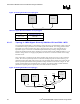
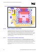
4.1.4.4. Topology 2A: Open Drain (OD) Signals Driven by ICH4-M – PWRGOOD
The Topology 2A OD signal PWRGOOD, which is driven by the ICH4-M (CMOS signal input to
processor) should adhere to the following routing and layout recommendations. Table 13 lists the
recommended routing requirements for the PWRGOOD signal of the processor. The routing guidelines
allow the signal to be routed as either micro-strip or strip-lines using 55 Ω ± 15% characteristic trace
impedance. The pull-up voltage for termination resistor Rtt is VCCP (1.05 V).
Note: The ICH4-M’s CPUPWRGD signal should be routed point-to-point to the processor’s PWRGOOD
signal. The routing from the processor’s PWRGOOD pin should fork out to both to the termination
resistor, Rtt, and the ICH4-M. Segments L1 and L2 from Table 13 should not T-split from a trace from
the pin.
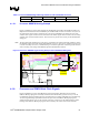
Figure 12. Routing Illustration for Topology 2A
CPU
ICH4-M
VCCP
L2
Rtt
L1