
Design Guide

Intel Pentium M/Celeron M Front Side Bus Design Guidelines
R
Intel
®
855GM/855GME Chipset Platform Design Guide 53
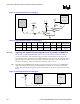
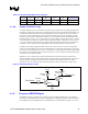
Table 13. Layout Recommendations for Topology 2A
L1
L2 Rtt Transmission Line Type
0.5” – 12.0” 0” – 3.0” 330 Ω ± 5% Micro-strip
0.5” – 12.0” 0” – 3.0” 330 Ω ±5% Strip-line
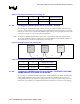
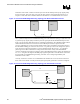
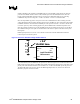
4.1.4.5. Topology 2B: CMOS Signals Driven by ICH4-M – DPSLP#
The Topology 2B CMOS DPSLP# signal, which is driven by the ICH4-M (CMOS signal input to the
processor), should adhere to the routing and layout recommendations illustrated in Figure 13. As listed
in Figure 13, the L1 and L2 segments of the DPSLP# signal topology can be routed as either micro-strip
or strip-lines using 55 Ω ± 15% characteristic trace impedance.
Note: The ICH4-M’s DPSLP# signal should be routed point-to-point with the daisy chain topology shown.
The routing of DPSLP# at the CPU should fork out to both the ICH4-M and the GMCH. Segments L1
and L2 from Figure 13 should not T-split from a trace from the pin.
Figure 13. Routing Illustration for Topology 2B
GMCH
L1
L2
ICH4-M
CPU
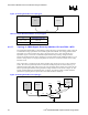
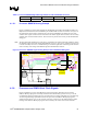
Table 14. Layout Recommendations for Topology 2B
L1 L2 Transmission Line Type
0.5” – 12.0” 0.5” – 6.5” Micro-strip
0.5” – 12.0” 0.5” – 6.5” Strip-line
4.1.4.6. Topology 2C: CMOS Signals Driven by ICH4-M – LINT0/INTR, LINT1/NMI,
A20M#, IGNNE#, SLP#, SMI#, and STPCLK#
The Topology 2C CMOS LINT0/INTR, LINT1/NMI, A20M#, IGNNE#, SLP#, SMI#, and STPCLK#
signals should implement a point-to-point connection between the ICH4-M and the processor. The
routing guidelines allow both signals to be routed as either micro-strip or strip-lines using 55 Ω ± 15%
characteristic trace impedance. No additional motherboard components are necessary for this topology.