
Design Guide

Intel Pentium M/Celeron M Front Side Bus Design Guidelines
R
54 Intel
®
855GM/855GME Chipset Platform Design Guide
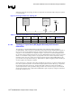
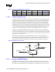
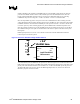
Figure 14. Routing Illustration for Topology 2C
CPU
ICH4-M
L1
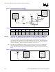
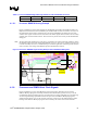
Table 15. Layout Recommendations for Topology 2C
L1 Transmission Line Type
0.5” – 12.0” Micro-strip
0.5” – 12.0” Strip-line
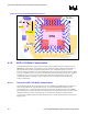
4.1.4.7. Topology 3: CMOS Signals Driven by ICH4-M to CPU and FWH – INIT#
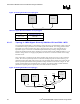
The signal INIT# should adhere to the following routing and layout recommendations. Table 16 lists the
recommended routing requirements for the INIT# signal of the ICH4-M. The routing guidelines allow
both signals to be routed as either micro-strip or strip-lines using 55 Ω ± 15% characteristic trace
impedance. Figure 15 shows the recommended implementation for providing voltage translation
between the ICH4-M’s INIT# voltage signaling level and any firmware hub (FWH) that utilizes a 3.3-V
interface voltage (shown as a supply V_IO_FWH). See Section 4.1.4.8 for more details on the voltage
translator circuit.
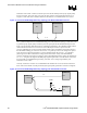
Series resistor Rs is a component of the voltage translator logic circuit and serves as a driver isolation
resistor. Rs is shown separated by distance L3 from the first bipolar junction transistor (BJT), Q1, to
emphasize the placement of Rs with respect to Q1. The placement of Rs a distance of L3 before the Q1
BJT is a specific implementation of the generalized voltage translator circuit shown in Figure 16. The
routing recommendations of transmission line L3 in Figure 15 is listed in Table 16 and Rs should be
placed at the beginning of the T-split of the trace from the ICH4-M’s INIT# pin.
Figure 15. Routing Illustration for Topology 3
CPU ICH4-M
L2
L3
L1
Rs
3.3V
3904
3904
FWH
L4
3.3V
Q1
Q2
R1
R2
V_IO_FWH