
Design Guide
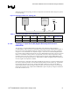

Intel Pentium M/Celeron M Front Side Bus Design Guidelines
R
Intel
®
855GM/855GME Chipset Platform Design Guide 55
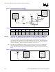
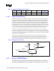
Table 16. Layout Recommendations for Topology 3
L1 + L2 L3 L4 Rs R1 R2 Transmission Line
0.5” – 12.0” 0” – 3.0” 0.5” – 6.0” 330 Ω ± 5% 1.3 kΩ ± 5% 330 Ω ± 5% Micro-strip
0.5” – 12.0” 0” – 3.0” 0.5” – 6.0” 330 Ω ± 5% 1.3 kΩ ± 5% 330 Ω ± 5% Strip-line
4.1.4.8. Voltage Translation Logic
A voltage translation circuit or component is required on any signals where the voltage signaling level
between two components connected by a transmission line may cause unpredictable signal quality. The
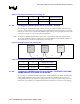
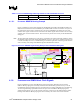
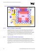
recommended voltage translation circuit for the platform is shown in Figure 16. The driver isolation
resistor, Rs, is place at the beginning of a transmission line that connects to the first bipolar junction
transistor, Q1. Though the circuit shown in Figure 16 was developed to work with signals that require
translation from a 1.05-V to a 3.3-V voltage level, the same topology and component values, in general,
can be adapted for use with other signals as well, provided the interface voltage of the receiver is also
3.3 V. Any component value changes or component placement requirements for other signals must be
simulated in order to guarantee good signal quality and acceptable performance from the circuit.
In addition to providing voltage translation between driver and receiver devices, the recommended
circuit also provides filtering for noise and electrical glitches. A larger first-stage collector resistor, R1,
can be used on the collector of Q1, however, it will result in a slower response time to the output falling
edge. In the case of the INIT# signal, resistors with value*s as close as possible to those listed in Figure
16 should be used without exception.
With the low 1.05-V signaling level of the Intel Pentium M / Intel Celeron M Front Side Bus, the
voltage translation circuit provides ample isolation of any transients or signal reflections at the input of
transistor Q1 from reaching the output of transistor Q2. Based on simulation results, the voltage
translation circuit can effectively isolate transients as large as 200 mV and that last as long as 60 ns.
Figure 16. Voltage Translation Circuit
1.3K ohm
+/- 5%
330 ohm
+/- 5%
3.3V
To Receive
r
From Driver
3904
3904
Q1
Q2
3.3V
Rs
R1
R2
330 ohm
+/- 5%
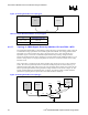
4.1.5. Processor RESET# Signal
The RESET# signal is a common clock signal driven by the GMCH CPURST# pin. In a production
system where no ITP700FLEX debug port is implemented, a simple point-to-point connection between
the CPURST# pin of the GMCH and processor RESET# pin is recommended (see Figure 17). On-die