
Design Guide

Intel Pentium M/Celeron M Front Side Bus Design Guidelines
R
56 Intel
®
855GM/855GME Chipset Platform Design Guide
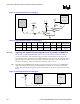
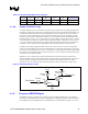
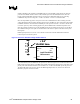
termination of the AGTL+ buffers on both the processor and the GMCH provide proper signal quality
for this connection. This is the same case as for the other common clock signals listed Section 4.1.2.
Length L1 of this interconnect should be limited to minimum of 1 inch and maximum of 6.5 inches.
Figure 17. Processor RESET# Signal Routing Topology with NO ITP700FLEX Connector
CPU
L1
GMCH
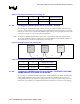
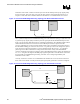
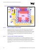
For a system that implements an ITP700FLEX debug port a more elaborate topology is required in order
to guarantee proper signal quality at both the processor signal pad and the ITP700FLEX input receiver.
In this case the topology illustrated in Figure 18 should be implemented. The CPURST# signal from the
GMCH should fork out (do not route one trace from GMCH pin and then T-split) towards the
processor’s RESET# pin as well as towards the Rtt and Rs resistive termination network placed next to
the ITP700FLEX debug port connector. Rtt (54.9 Ω + 1%) pulls-up to the VCCP voltage and is placed
at the end of the L2 line that is limited to a 12-inch maximum length. Rs (22.6 Ω +/- 1%) should be
placed right next to Rtt to minimize the routing between them in the vicinity of the ITP700FLEX
connector to limit the L3 length to less than 0.5 inches. ITP700FLEX operation requires the matching of
L2 + L3 - L1 length to the length of the BPM[4:0]# signals length within ± 250 mils. Refer to Section 0
for more details on ITP700FLEX signal routing. See Table 17 for routing length summary and
termination resistor values.
Currently 1% tolerance resistors are recommended for Rs and Rtt. The use of 5% tolerant resistors for
these resistors and whether it could provide adequate signal quality performance is under investigation.
Figure 18. Processor RESET# Signal Routing Topology with ITP700FLEX Connector
CPU
L2
L3
Rs
L1
ITPFLEX
CONNECTOR
GMCH
Rtt
VCCP
RESET#
CPURESET#
RESET#