
Design Guide

Intel Pentium M/Celeron M Front Side Bus Design Guidelines
R
58 Intel
®
855GM/855GME Chipset Platform Design Guide
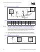
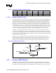
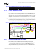
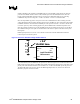
BCLK[1:0] layer transition vias are accompanied by GND stitching vias. For similar reasons, routing for
the ITP interposer’s BCLK[1:0] signals also transition from Layer 3 to the secondary side layer and have
507-mil long traces on this layer. Throughout the routing length on Layer 3, BCLK[1:0] signals should
reference a solid GND plane on Layer 2 and Layer 4 as shown in Figure 8.
If a system supports either the on-board ITP700FLEX connector or ITP Interposer only, then differential
host clock routing to either the ITP700FLEX connector or CPU socket (but not both) is required.
Figure 20. Processor and GMCH Host Clock Layout Routing Example
Secondary
Side
GMCH
CPU
FROM
CK
-
408
GMCH
BCLK
[
1:0
]
ITP
FLEX
CPU
BCLK[1:0]
ITP
BCLK[1:0]
ITP
Interposer
BCLK[1:0]
GND VIA
Layer3
4.1.7. Processor GTLREF Layout and Routing Recommendations
There is one AGTL+ reference voltage pin on the Intel Pentium M / Intel Celeron M processor,
GTLREF, which is used to set the reference voltage level for the AGTL+ signals (GTLREF). The
reference voltage must be supplied to the GTLREF pin. The voltage level that needs to be supplied to
GTLREF must be equal to 2/3 * VCCP ± 2%. The GMCH also requires a reference voltage