
Design Guide

Intel Pentium M/Celeron M Front Side Bus Design Guidelines
R
60 Intel
®
855GM/855GME Chipset Platform Design Guide
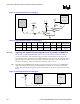
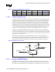
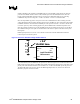
Figure 22. Processor GTLREF Motherboard Layout
PRIMARY SIDE
Pin G1
Pin AG1
GTLREF
Zo =55
Ω
<0.5”
R2
VCCP
Pin E26
Banias
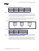
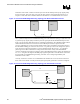
Pin G1
Pin AG1
Pin AG1
GTLREF GTLREF
R1 R1
R2
VCCP
Pin E26 Pin E26
CPU
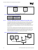
4.1.8. AGTL+ I/O Buffer Compensation
The Intel Pentium M / Intel Celeron M processor has 4 pins, COMP[3:0], and the GMCH has 2 pins,
HRCOMP[1:0], that require compensation resistors to adjust the AGTL+ I/O buffer characteristics to
specific board and operating environment characteristics. Also, the GMCH requires two special
reference voltage generation circuits to pins HSWNG[1:0] for the same purpose described above. Refer
to the Intel
®
Pentium
®
M Processor Electrical, Mechanical, and Thermal Specification, Intel
®
Pentium
®
M (90nm process) Processor Electrical, Mechanical, and Thermal Specification, and RS – Intel
®
855GM/GME (Montara-GM/GM+) Chipset GMCH External Design Specification for details on
resistive compensation.
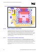
4.1.8.1. Processor AGTL+ I/O Buffer Compensation
For the Intel Pentium M / Intel Celeron M processor, the COMP[2] and COMP[0] pins (see Figure 23)
must each be pulled-down to ground with 27.4 Ω ± 1% resistors and should be connected to the
processor with a Zo = 27.4 Ω trace that is less than 0.5 inches from the processor pins. The COMP[3]
and COMP[1] pins (see Figure 24) must each be pulled-down to ground with 54.9 Ω ± 1% resistors and
should be connected to the processor with a Zo = 55 Ω trace that is less than 0.5 inches from the
processor pins. COMP[3:0] traces should be at least 25 mils (> 50 mils preferred) away from any other
toggling signal.