
Design Guide

Intel Pentium M/Celeron M Front Side Bus Design Guidelines
R
Intel
®
855GM/855GME Chipset Platform Design Guide 61
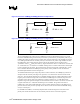
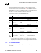
Figure 23. Processor COMP[2] & COMP[0] Resistive Compensation
27.4
Ω
+/- 1%
COMP[0]
27.4
Ω
+/- 1%
COMP[2]
Figure 24. Processor COMP[3] & COMP[1] Resistive Compensation
54.9
Ω
+/- 1%
COMP[3]
54.9
Ω
+/- 1%
COMP[1]
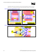
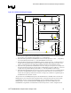
The recommended layout of the processor COMP[3:0] resistors is illustrated in Figure 25. To avoid
interaction with PSB routing on internal layers and VCCA power delivery on the primary side, Layer 1,
COMP[1:0] resistors are placed on the secondary side. Ground connections to the COMP[1:0] resistors
use a small ground flood on the secondary side layer and connect only with a single GND via to stitch
the GND planes. The compact layout as shown in Figure 25 should be used to avoid excessive
“perforation” of the V
CCP
plane power delivery. Figure 25 illustrates how a 27.4 Ω resistor connects with
an ~18-mil wide (Zo = 27.4 Ω) trace to COMP0. Necking down to 14 mils is allowed for a short length
to pass in between the dog bones. The 54.9-Ω resistor connects with a regular 5-mil wide (Zo = 55 Ω)
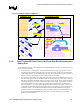
trace to COMP1. Placement of COMP[1:0] on the primary side is possible as well. An alternative
placement implementation is shown in Figure 26.
To minimize motherboard space usage and produce a robust connection, the COMP[3:2] resistors are
also placed on the secondary side (Figure 25, right side). A 27.4-Ω resistor connects with an 18-mil
wide (Zo = 27.4 Ω) and 260-mil long trace to COMP2. Necking down to 14 mils is allowed for a short
length to pass in between the dog bones. Notice that the COMP2 (Figure 25, left side) dog bone trace
connection on the primary side is also widened to 14 mils to meet the Zo = 27.4-Ω characteristic
impedance target. The right side of Figure 25 also illustrates how the 54.9 Ω ± 1% resistor connects with
a regular 5-mil wide (Zo = 55Ω) and 100-mil long trace to COMP3. The ground connection of
COMP[3:2] is done with a small flood plane on the secondary side that connects to the GND vias of
pins AA1 and Y2 of the processor pin-map. This is done to avoid via interaction with the PSB routing
on Layer 3 and Layer 6.
For COMP2 and COMP0, it is extremely important that 18-mil wide dog bone connections on the
primary side and 18-mil wide traces on the secondary sides be used to connect the signals to