
Design Guide

Intel Pentium M/Celeron M Front Side Bus Design Guidelines
R
64 Intel
®
855GM/855GME Chipset Platform Design Guide
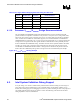
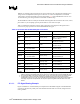
Table 18. ITP Signal Default Strapping When ITP Debug Port Not Used
Signal Resistor Value Connect To Resistor Placement
TDI 150 Ω ± 5% VCCP Within 2.0” of the CPU
TMS 39 Ω ± 5% VCCP Within 2.0” of the CPU
TRST# 680 Ω ± 5% GND Within 2.0” of the CPU
TCK 27 Ω ± 5% GND Within 2.0” of the CPU
TDO Open NC N/A
4.1.10. Processor V
CCSENSE
/V
SSSENSE
Design Recommendations
The VCCSENSE and VSSSENSE signals of the Intel Pentium M processor and Intel Celeron M
provide isolated, low impedance connections to the processor’s core power (VCC) and ground (VSS).
These pins can be used to sense or measure power (VCC) or ground (VSS) near the silicon with little
noise. To make them available for measurement purposes, it is recommended that VCCSENSE and
VSSSENSE both be routed with a Zo = 55 Ω ± 15% trace of equal length. Use 3:1 spacing between the
routing for the two signals and all other signals should be a minimum of 25 mils (preferably 50 mils)
from VCCSENSE and VSSSENSE routing. Terminate each line with an optional (default is No Stuff)
54.9 Ω ± 1% resistor. Also, a ground via spaced 100 mils away from each of the test point vias for
VCCSENSE and VSSSENSE should be added. A third ground via should also be placed in between
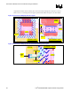
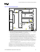
them to allow for a differential probe ground. See Figure 28 for the recommended layout example.
Figure 28. V
CCSENSE
/V
SSSENSE
Routing Example
4.2. Intel System Validation Debug Support
In any PC design, it is critical to enable industry-standard tools to allow for debug of a wide range of
issues that come up in the normal design cycle. In a mobile design, electrical/logic visibility is very
limited, often making progress on debugging such issues very time consuming. In some cases progress it
not possible without board re-design or extensive rework. The following sections describe the three
debug capabilities: ITP, LAI, and ODLAT.