
Design Guide

Intel Pentium M/Celeron M Front Side Bus Design Guidelines
R
66 Intel
®
855GM/855GME Chipset Platform Design Guide
1. Provide a motherboard with a CPU socket. The FSB LAI is an interposer that plugs into the CPU
socket, and the CPU then plugs into the LAI. The use of non-standard sockets may also prohibit
the LAI from working as the locking mechanism may become inaccessible. It is important to
check the LAI design guidelines to ensure a particular socket will work. Note that the LAI was
designed to accommodate the most common (and at the time the only known) processor sockets
on the market.
2. Observe FSB LAI keepout requirements. There are several options to achieving this. For example
removing the motherboard from the case (typically the first step to meeting keepout requirements)
or relocating any components that would otherwise be in the keepout area for debug purposes (i.e.
axial lead devices that can be de-soldered and re-soldered to the other side of the board, parts that
can be removed and blue-wired further away, etc.). If keepouts still cannot be met, Intel strongly
recommends that a separate debug motherboard be built which has the same bill of material
(BOM) and Netlist, but with FSB LAI keepout requirements met (this also gives the opportunity
to add other test-points).
4.2.2.2. Implementation
Details from Agilent Corporation on the FSB LAI mechanicals (i.e. design guide with keepout volume
info) are available for ordering. Please contact your local Intel field representative on how to obtain the
latest design info. See Section 4.3.3 for more details.
4.2.3. Intel Pentium M / Intel Celeron M Processor On-Die Logic
Analyzer Trigger (ODLAT) Support
The Intel Pentium M / Intel Celeron M processor provides support for 3 address/data recognizers on-die
for setting on-die logic analyzer triggers (ODLAT) or breakpoints. Details from American Arium* on
the ODLAT are currently available for ordering.
4.3. Onboard Debug Port Routing Guidelines
For systems incorporating the Intel Pentium M / Intel Celeron M processor, the debug port should be
implemented as either an onboard debug port or via an interposer. Please reference the document
ITP700 Debug Port Design Guide, which can be found on
http://www.intel.com/design/Xeon/guides/24967912.pdf
, for the most up to date information
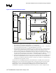
4.3.1. ITP Signal Routing Guidelines
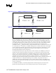
Figure 29 illustrates recommended connections between the onboard ITP700FLEX debug port,
processor, GMCH, and CK-408 clock chip in the cases where the debug port is used.