
Design Guide

Intel Pentium M/Celeron M Front Side Bus Design Guidelines
R
68 Intel
®
855GM/855GME Chipset Platform Design Guide
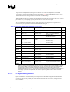
termination guarantee proper signal quality for the BPM[4:0]# signals. Due to the length of the
ITP700FLEX cable, the length L2 of the BPM[4:0]# signals on the motherboard should be limited to be
shorter than 6.0 inches. The BPM[4:0]# signals’ length L2 should be length matched to each other
within ± 250 mils. The BPM[4:0]# signal trace lengths are matched inside the processor package, thus
motherboard routing does not need to compensate for any processor package trace length mismatch.
Due to the processor’s AGTL+ on-die termination for BPM[3:0]# and PRDY#, there is no issue or
concern if the BPM[4:0]# pins of the ITP700FLEX connector are left floating when the ITP is not being
used and the ITP700FLEX cable is unplugged.
Route the ITP700FLEX connector’s BPM[5]# signal as a Zo = 55 Ω point-to-point connection to the
processor’s PREQ# pin. Integrated on the ITP700FLEX BPM[5]# driver signal is a resistive pull-up that
guarantees proper signal quality at the processor’s PREQ# input pin. The processor has an integrated,
weak, on-die pull-up to VCCP for the PREQ# signal to guarantee a proper logic level when the
ITP700FLEX port connector is not plugged in. There is no need for any external termination on the
motherboard for the BPM[5]# = PREQ# signal. The maximum length of BPM[5]#/PREQ# should not
exceed 6.0 inches.
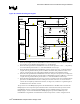
As explained in Sections 4.1.5, the RESET# signal forks (see Figure 17) out from the GMCH’s
CPURST# pin and is routed to the processor and ITP700FLEX debug port. One branch from the fork
connects to the processor’s RESET# pin and the second branch connects to a 220 W ± 5% termination
pull-up resistor to VCCP placed close to the ITP700FLEX debug port. A series 22.6 W ± 1% resistor is
used to continue the path to the ITP700FLEX RESET# pin with the RESETITP# net in Figure 28. The
length of the RESETITP# net (labeled as net L4) should be limited to be less than 0.5 inches.
There is no need for pull-up termination on the processor side of the RESET# net due to presence of
AGTL+ on-die termination on the processor and the GMCH.
The ITP700FLEX debug port’s BCLK/BCLK# inputs are driven with a 100-MHz differential clock
from the CK-408 clock chip. The CK-408 also feeds another two pairs of 100-MHz differential clocks
to the processor BCLK[1:0] and the GMCH BCLK[1:0] input pins. Common clock signal timing
requirements of the GMCH and the processor requires matching of processor and GMCH BCLK[1:0]
nets L6 and L7, respectively. To guarantee correct operation of ITP700FLEX, the BCLK/BCLK# net L8
should be tuned to be within ± 250mils to the sum of length L6 of the BCLK[1:0] lines and the
additional length L2 of the BPM#[4:0] signals.
i.e. L6 + L2 = L8 (within ± 250mils).
The timing requirements for the BPM[5:0]#, RESET#, and BCLK/BCLK# signals of the ITP700FLEX
debug port requires careful attention to their routing. Standard high frequency bus routing practices
should be observed.
1. Keep a minimum of 2:1 spacing in between these signals and to other signals.
2. Reference these signals to ground planes and avoid routing across power plane splits.
3. The number of routing layer transitions should be minimized. If layout constraints require a
routing layer transition, any such transition should be accompanied with ground stitching vias
placed within 100 mils of the signal via with at least one ground via for every two signals making
a layer transition.
DBR# should be routed to the system reset logic (e.g. the SYSRST# signal of the ICH4-M) and initiate
the equivalent of a front panel reset commonly found in desktop systems. The 150 Ω to 240 Ω pull-up
resistor should be placed within 5.5” of the ITP700FLEX connector. Note that the CPU should not be
power cycled when DBR# is asserted.