
Design Guide

Intel Pentium M/Celeron M Front Side Bus Design Guidelines
R
Intel
®
855GM/855GME Chipset Platform Design Guide 69
DBA# is an optional system signal that can be used to indicate to the system that the ITP/TAP port is
being used. If not implemented, this signal can be left as no connect. If implemented, it should be
routed with a 150 Ω to 240 Ω pull-up resistor placed within 5.5” of the ITP700FLEX connector. See
the ITP700 Debug Port Design Guide for more details on DBA# usage.
The ITP700FLEX VTT and VTAP pins should be shorted together and connected to the VCCP (1.05 V)
plane with a 0.1-µF decoupling capacitor placed within 0.1 inch of the VTT pins.
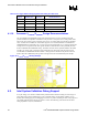
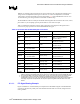
Table 19 summarizes termination resistors values, placement, and voltages the ITP signals need to
connect to for proper operation for onboard ITP700FLEX debug port.
Table 19. Recommended ITP700FLEX Signal Terminations
Signal Termination Value Termination Voltage Termination/Decap Location Notes
TDI
150
Ω ± 5%
VCCP (1.05 V)
Within
± 1.5” of the CPU TDI pin
3
TMS
39.2
Ω ± 1%
VCCP (1.05 V)
Within
± 1” of the ITP700FLEX
connector TMS pin
3
TRST#
510 – 680
Ω ± 5%
GND
Anywhere between CPU and
ITP700FLEX connector
3
TCK
27.4
Ω ± 1%
GND
Within
± 1” of the ITP700 FLEX
connector TCK pin
3
TDO
54.9
Ω ± 1% pull-up and 22.6
Ω ± 1% series resistor
VCCP (1.05 V)
Within 1” of the ITP700FLEX
connector TDO pin
3
BCLK(p/n)
FBO Connect to TCK pin of CPU N/A N/A
RESET#
220
Ω ± 5% pull-up and 22.6
Ω ± 1% series resistor
VCCP (1.05 V)
Within 0.5” of the ITP700FLEX
connector RESET# pin
3
BPM[5:0]# Not Required 1
DBA#
150-240
Ω ± 5%
VCC of target system
recovery circuit.
Within 5.5” of the ITP700FLEX
connector DBA# pin
2
DBR#
150-240
Ω ± 5%
VCC of target system
recovery circuit
Within 5.5” of the ITP700FLEX
connector DBR# pin
VTAP Short to VCCP plane VCCP (1.05 V)
VTT Short to VCCP plane VCCP (1.05 V)
Add 0.1-µF decap within 0.1 inch of
VTT pins of ITP700FLEX connector
NOTES:
1. All the needed terminations to guarantee proper signal quality are integrated inside the processor AGTL+
buffers or inside the ITP700FLEX debug port. No need for any external components for the BPM[5:0]# signals.
2. Only required if DBA# is used with any target system circuitry. This signal may be left unconnected if unused.
3. In cases where a system is designed to utilize the ITP700FLEX debug port for debug purposes but the
ITP700FLEX connector may or may not be populated at all times although the signal routing and termination or
decoupling components are implemented, the component placement guidelines should adhere to the ones
listed in.
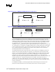
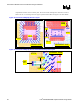
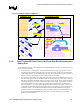
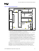
4.3.1.1. ITP Signal Routing Example
Figure 30 illustrates a recommended layout example for the ITP700FLEX signals. The ITP700FLEX
connector is placed on the primary side of the motherboard and results in a smooth, straight-forward
routing solution.