
Design Guide

Intel Pentium M/Celeron M Front Side Bus Design Guidelines
R
70 Intel
®
855GM/855GME Chipset Platform Design Guide
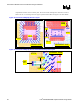
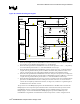
Note that the V
CCP
(1.05 V) power delivery continues from the processor socket cavity on the secondary
side of the motherboard through the pin field as shown on the right side of Figure 30. Three V
CCP
vias in
conjunction with three ground stitching vias allow a transition to the primary side to connect to the VTT
and VTAP pins of the ITP700FLEX connector and also a transition back to the secondary side of the
motherboard. A small V
CCP
flood is created on the secondary side under the body of the ITP700FLEX
connector with a 0.1-µF decoupling capacitor. This also provides a convenient connection for the 220-Ω
pull-up for RESET#, the 54.9-Ω pull-ups for TDO, as well as the 39.2-Ω pull-up for the TMS signal.
Notice the very short trace from the 22.6-Ω series resistors for the RESET# and TDO signals to the
ITP700FLEX pins. See also Section 4.1.5 for more details on RESET# signal routing.
The 150-Ω TDI pull-up is connected to the V
CCP
(1.05 V) flood on the secondary side close to processor
pin.
The ITP700FLEX TCK pin has a 27.4-Ω pull-down to ground very close to the ITP700FLEX connector
and also routes to the processor’s TCK pin and loops back with no stub to the FBO pin of the
ITP700FLEX connector.
BCLK/BCLK# are routed in this example on Layer 3. For more BCLK/BCLK# routing details, refer to
Figure 20 in Section 4.1.6.
4.3.1.2. ITP_CLK Routing to ITP700FLEX Connector
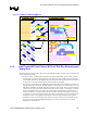
A layout example for ITP_CLK/ITP_CLK# routing to an ITP700FLEX connector is shown in Figure
30. The CK-408 clock chip is mounted on the primary side of the motherboard and the differential clock
pair also breaks out on the same side. The differential ITP clock pair routing requires the use of a pair of
33-Ω ± 5% series resistors placed within 0.5 inches of the clock chip output pins followed by a pair of
49.9-Ω ± 1% termination resistors to ground. The ITP_CLK/ITP_CLK# signals are routed as a
differential pair from the junction of the 33-Ω and 49.9-Ω ± 5% resistors across the internal Layer 6
through an open channel to the ITP700FLEX connector. Serpentining of the ITP_CLK traces is also
performed in order to meet the ± 250 mils length matching requirement between ITP_CLK and the sum
of length L6 of the BCLK[1:0] lines and the additional length L2 of the BPM#[5:0] signals in Figure 29.
The ITP_CLK pair routing then switches back to the primary side layer through a via near the
ITP700FLEX connector.