
Design Guide

Intel Pentium M/Celeron M Front Side Bus Design Guidelines
R
Intel
®
855GM/855GME Chipset Platform Design Guide 73
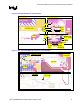
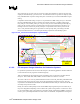
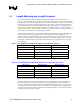
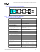
also requires the use of a pair of 33-Ω ± 5% series resistors placed within 0.5 inches of the clock chip
output pins and followed by a pair of 49.9-Ω ± 1% termination resistors to ground. The majority of the
ITP_CLK differential serpentine routing takes place on internal Layer 6 below the PSB address signal
routing.
Completion of ITP+CLK routing on Layer 6 is not possible due to PSB routing on Layer 6. Therefore
the ITP_CLK differential pair then is routed to the secondary side layer to complete routing to the
ITP_CLK (pin A16) and ITP_CLK# (pin A15) pins of the processor while matching the BCLK[1:0]
routing on the secondary side for a 507-mil length (see Figure 20 and description in Section 4.1.6).
Routing to the CPU socket on the primary side layer is not possible because of the presence of the
VCCA 1.8V plane flood along the A-signal side row of the pin-map. ITP_CLK routing to the ITP
interposer should achieve the ± 250 mil length matching requirement of the BCLK[1:0] lines.
Figure 32. ITP_CLK to CPU ITP Interposer Layout Example
PRIMARY SIDE
LAYER 6
SECONDARY
SIDE
ITP_CLK
ITP_CLK#
A16, A15 pins
CK-408
33Ω
49.9Ω
PRIMARY SIDE
LAYER 6
SECONDARY
SIDE
ITP_CLK
ITP_CLK#
A16, A15 pins
CK-408
33Ω
49.9Ω
4.3.2.2. ITP Interposer Design Guidelines for Production Systems
For production systems that do not use the ITP interposer, the following guidelines should be followed
to ensure that all necessary signals are terminated properly.
Table 18 summarizes all the signals that require termination when a system does not utilize the ITP
interposer. This includes TDI, TMS, TRST#, and TCK. TDO can be left as a no connect.
The series 33 Ω and 49.9 Ω ±1% parallel termination resistors on the ITP_CLK/ITP_CLK# differential
host clock inputs to the processor socket can also be depopulated for production systems. The only
requirement is that the BIOS should disable the third differential host clock pair routed from the CK-408
clock chip to the processor socket.
Finally, the 150 Ω to 240 Ω pull-up resistor for the DBR# output signal from processor socket may or
may not be depopulated depending on how it affects the system reset logic that it is connected to. Thus,
it is the responsibility of the system designer to determine whether termination for DBR# is required or
not for a given system implementation. The same is also true for DBA#, if implemented. This signal is