
Design Guide

System Memory Design Guidelines (DDR-SDRAM) for SO-DIMM configuration
R
Intel
®
855GM/855GME Chipset Platform Design Guide 77
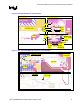
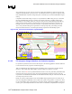
6.1. Length Matching and Length Formulas
The routing guidelines presented in the following subsections define the recommended routing
topologies, trace width and spacing geometries, and absolute minimum and maximum routed lengths for
each signal group, which are recommended to achieve optimal SI and timing. In addition to the absolute
length limits provided in the individual guideline tables, more restrictive length matching formulas are
also provided which further restrict the minimum to maximum length range of each signal group with
respect to clock, within the overall boundaries defined in the guideline tables, as required to guarantee
adequate timing margins. These secondary constraints are referred to as length matching constraints and
the formulas used are referred to as length matching formulas.
All signal groups except the clocks and feedback signals are length matched per slot to the DDR clocks,
with the clocks themselves being length tuned to a fixed length across each SO-DIMM slot. The
amount of minimum to maximum length variance allowed for each group around the clock reference
length varies from signal group to signal group depending on the amount of timing variance which can
be tolerated. A simple summary of the length matching formulas for each signal group is provided in
the tables below.
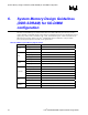
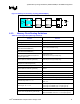
Table 21. Intel 855GM Chipset GMCH DDR 200/266 Length Matching Formulas
Signal Group Minimum Length Maximum Length
Control to Clock Clock –1.0” Clock + 0.5”
Command to Clock Clock – 1.0” Clock + 2.0”
CPC to Clock Clock – 1.0” Clock + 0.5”
Strobe to Clock Clock – 1.0” Clock + 0.5”
Data to Strobe Strobe – 25 mils Strobe + 25 mils
NOTE: All length matching formulas are based on GMCH die-pad to SO-DIMM connector pin total length.
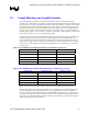
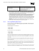
Table 22. Intel 855GME Chipset GMCH DDR 200/266/333 Length Matching Formulas
Signal Group Minimum Length Maximum Length
Control to Clock Clock –2.0” Clock - 0.5”
Command to Clock Clock – 2.0” Clock + 2.0”
CPC to Clock Clock – 2.0” Clock - 1.0”
Strobe to Clock Clock – 2.0” Clock + 0.5”
Data to Strobe Strobe – 25 mils Strobe + 25 mils
NOTE: All length matching formulas are based on GMCH die-pad to SO-DIMM connector pin total length.
Package length tables are provided for all signals in order to facilitate this pad to pin matching. Note
that the clock length used for length matching may vary by SO-DIMM slot, based on SO-DIMM
spacing. Length formulas should be applied to each SO-DIMM slot independently. An offset of up to
1.0” between clock groups is allowed under the guidelines. The full geometry and routing guidelines
along with the exact length matching formulas and associated diagrams are provided in the individual
signal group guidelines sections to follow.