
Design Guide

System Memory Design Guidelines (DDR-SDRAM) for SO-DIMM configuration
R
80 Intel
®
855GM/855GME Chipset Platform Design Guide
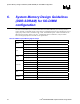
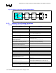
Parameter Definition
Breakout Exceptions
(Reduced geometries for GMCH breakout region)
Inner Layers: 4 mil trace, 4 mil pair space allowed
Outer Layers: 5 mil trace, 5 mil pair space allowed
Pair to pair spacing of 5 mils allowed
Spacing to other DDR signals of 5 mils allowed
Maximum breakout length is 0.3”
NOTES:
1. Pad to Pin length tuning is utilized on clocks in order to achieve minimal variance. Package lengths range
between approximately 600 mils and 1400 mils. Exact package lengths for each clock signal are provided at
the end of this Section. Overall target length should be established based on placement and routing flow. The
resulting motherboard segment lengths must fall within the ranges specified.
2. The DDR clocks should be routed on internal layers, except for pin escapes. It is recommended that pin escape
vias be located directly adjacent to the ball pads on all clocks. Surface layer routing should be minimized.
3. Clock differential impedance is controlled indirectly through the single ended impedance specification for the
board. Clock signal integrity and edge rates are improved when clock trace widths are widened from the
standard 55
Ω single ended trace width. As the table indicates, a trace width of approximately 3 mils wider than
standard width was found to be optimal (i.e. inner layers: 4mils std + 3mils = 7mils). The nominal single ended
impedance of the widened clock traces is in the range of 42
Ω, and the nominal differential impedance is in the
range of 70
Ω. However, impedance control is implemented through geometry control; these values are for
reference only.
4. Exceptions to the trace width and spacing geometries are allowed in the breakout region in order to fan-out the
interconnect pattern. Reduced spacing should be avoided as much as possible.
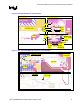
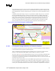
6.3.3.1. Clock Length Matching Requirements
The GMCH chipset provides three differential clock pair for each SO-DIMM. A differential clock pair
is made up of a SCK signal and its complement signal SCK#. Refer to Section 6.1 for more details on
length matching requirements.
The differential pairs for one SO-DIMM are:
SCK[0] / SCK#[0]
SCK[1] / SCK#[1]
SCK[2] / SCK#[2]
The differential pairs for the second SO-DIMM are:
SCK[3] / SCK#[3]
SCK[4] / SCK#[4]
SCK[5] / SCK#[5]
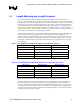
The two sets of differential clocks must be length tuned on the motherboard such that any pair to pair
package length variation is tuned out. The three pairs associated with SO-DIMM0 are tuned to a fixed
overall length, including package, and the three pairs associated with SO-DIMM1 are tuned to a fixed
overall length.
The two traces associated with each clock pair are length matched within the package; however some
additional compensation may be required on the motherboard in order to achieve the ± 10 mil length
tolerance within the pair.
Between clock pairs the package length varies substantially. Therefore, the motherboard length of each
clock pair must be length adjusted to tune out package variance. The total length including package
should be matched to within ± 25 mils of each other, as shown in Figure 34. This may result in a clock
length variance of as much as 700 mils on the motherboard.
The first step in determining the routing lengths for clocks and all other clock relative signal groups is to
establish the target length for each SO-DIMM clock group. These target lengths are shown as X0 and