
Design Guide

System Memory Design Guidelines (DDR-SDRAM) for SO-DIMM configuration
R
82 Intel
®
855GM/855GME Chipset Platform Design Guide
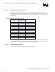
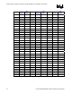
6.3.3.3. Clock Package Length Table
The package length data in the table below should be used to tune the motherboard length of each
SCK/SCK# clock pair between the GMCH and the associated SO-DIMM socket. It is recommended
that die-pad to SO-DIMM pin length be tuned to within ± 25 mils in order to optimize timing margins
on the interface.
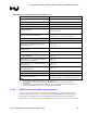
Table 25. Memory Clock Package Lengths
Signal Pin Number
Package Length
(mils)
SCK_0 AB2 1177
SCK#_0 AA2 1169
SCK_1 AC26 840
SCK#_1 AB25 838
SCK_2 AC3 1129
SCK#_2 AD4 1107
SCK_3 AC2 1299
SCK#_3 AD2 1305
SCK_4 AB23 643
SCK#_4 AB24 656
SCK_5 AA3 1128
SCK#_5 AB4 1146
Package length compensation can be performed on each individual clock output thereby matching total
length on SCK/SCK# exactly, or alternatively the average package length can be used for both outputs
of a pair and length tuning done with respect to the motherboard portion only.
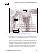
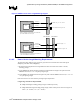
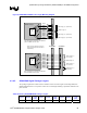
6.3.3.4. Clock Routing Example
Figure 35 is an example of a board routing for the clock signal group.