
Design Guide

System Memory Design Guidelines (DDR-SDRAM) for SO-DIMM configuration
R
Intel
®
855GM/855GME Chipset Platform Design Guide 83
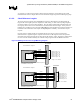
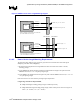
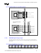
Figure 35. Clock Signal Routing Example
GMCH
SODIMM0
SODIMM1
Clocks
6.3.4. Data Signals – SDQ[71:0], SDM[8:0], SDQS[8:0]
The GMCH data signals are source synchronous signals that include a 72-bit wide data bus, which
includes 8 check bits for Error Checking and Correction (ECC), a set of 9 Data Mask bits, and a set of 9
data strobe signals. There is an associated data strobe and data mask bit for each of the 8-bit data byte
groups, making for a total of nine – 10-bit byte lanes. This section summarizes the SDQ/SDM to SDQS
routing guidelines and length matching recommendations.
The data signals include SDQ[71:0], SDM[8:0], and SDQS[8:0]. The data signals should transition from
an external layer to an internal signal layer under the GMCH. The data signals should keep to the same
internal layer until transitioning back to an external layer at the series resistor. After the series resistor,
the signal should transition from the external layer to the same internal layer and route to SO-DIMM0.
At SO-DIMM0, the signal should transition to an external layer and connect to the appropriate pad of
the connector. After the SO-DIMM0 transition, continue to route the signal on the same internal layer to
SO-DIMM1, then transition the signal back out to an external layer and connect to the appropriate pad
of SO-DIMM1. Connection to the termination resistor should be via the same internal layer with a
transition back to the external layer near the resistor. External trace lengths should be minimized.