
Design Guide

System Memory Design Guidelines (DDR-SDRAM) for SO-DIMM configuration
R
Intel
®
855GM/855GME Chipset Platform Design Guide 85
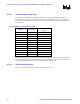
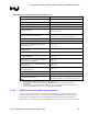
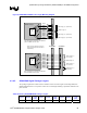
Table 26. Memory Data Signal Group Routing Guidelines
Parameter Definition
Signal Group SDQ[71:0], SDQS[8:0], SDM[8:0]
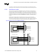
Motherboard Topology Daisy Chain with Parallel Termination
Reference Plane Ground Referenced
Characteristic Trace Impedance (Zo) 55 Ω +/- 15%
Nominal Trace Width
Inner layers: 4 mils
Outer layers: 5 mils
Minimum Spacing to Trace Width Ratio
SDQ/SDM: 2 to 1 (e.g. 8 mil space to 4 mil trace)
SDQS: 3 to 1 (e.g. 12 mil space to 4 mil trace)
Minimum Isolation Spacing to non-DDR Signals 20 mils
Package Length P1 700 mils +/- 300 mils (See Table 28 for details)
Trace Length L1 – GMCH Signal Ball to Series
Termination Resistor Pad
Min = 0.5”
Max = 3.75”
Trace Length L2 – Series Termination Resistor Pad to
First SO-DIMM Via
Max = 0.75”
Stub Length S0, S1 – Stub from Via to SO-DIMM Pad Max = 0.25”
Total Length L1 + L2 + S0 – Total Length from GMCH
to First SO-DIMM Pad
Min = 0.5”
Max = 4.0”
Total Length L1 + L2 + L3 + S1 – Total Length from
GMCH to Second SO-DIMM Pad
Min = 0.75”
Max = 4.5”
Total Length S0 + L3 + S1– Total SO-DIMM pad to SO-
DIMM pad spacing
Min = 0.25”
Max = 1.0”
Trace Length L4 – Last SO-DIMM Via to Parallel
Termination Resistor Pad
Max = 1.0”
Series Termination Resistor (Rs) 10 Ω ± 5%
Parallel Termination Resistor (Rt) 56 Ω ± 5%
Length Matching Requirements
SDQS to SCK/SCK# See length matching Section 6.3.4.2
SDQ/SDM to SDQS, to +/- 25mils, within each byte lane
NOTES:
1. Power distribution vias from Rt to Vtt are not included in this count.
2. The overall minimum and maximum length to the SO-DIMM must comply with clock length matching
requirements.
3. It is possible to route using 4 vias if trace segments L2 and L4 are routed on the same external layer as the
associated SO-DIMM, for example if L2 is on the same layer as SO-DIMM0.
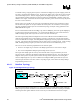
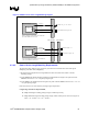
6.3.4.2. SDQS to Clock Length Matching Requirements
The first step in length matching is to determine the SDQS length range based on the SCK/SCK#
reference length defined previously. The total length of the SDQS strobe signals, including package
length, between the GMCH die-pad and the SO-DIMMs must fall within the range defined in the
formulas below. See the clock Section for the definition of the clock reference length. Refer to Figure