
Design Guide

System Memory Design Guidelines (DDR-SDRAM) for SO-DIMM configuration
R
Intel
®
855GM/855GME Chipset Platform Design Guide 87
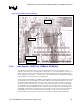
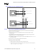
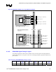
Figure 37. SDQS to Clock Trace Length Matching Diagram
SO-DIMM0
GMCH Package
GMCH
Die
SDQS[8:0]
SCK[2:0]
SCK#[2:0]
Note: All lengths are measured from GMCH die-
pad to SO-DIMM connector pad.
SDQS Len
g
th = Y0 , where
Clock Reference Length = X0
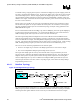
SO -DIMM0 SO-DIMM 1
GMCH Package
SDQS[8:0]
SCK[5:3]
SCK#[5:3]
Clock Ref. Length = X1
Note: All lengths are measured from GMCH die-
p
ad to SO-DIMM connector
p
ad.
SDQS Length = Y1
GMCH
Die
6.3.4.3. Data to Strobe Length Matching Requirements
The data bit signals, SDQ[71:0] are grouped by byte lanes and associated with a data mask signal
SDM[8:0], and a data strobe, SDQS[8:0].
• The data and mask signals must be length matched to their associated strobe within ± 25 mils,
including package.
• For SO-DIMM0 this length matching includes the motherboard trace length to the pads of the SO-
DIMM0 connector (L1 + L2 + S0) plus package length.
• For SO-DIMM1, the motherboard trace length to the pads of the SO-DIMM1 connector (L1 + L2 + L3
+ S1) plus package length.
Refer to Section 6.2 for more details on package length compensation.
Length range formula for SDQ and SDM,
X = SDQS total length, including package length, as defined previously
Y = SDQ, SDM total length, including package length, within same byte lane as show in Figure 38,
where: ( X – 25 mils ) ≤ Y ≤ ( X + 25 mils )