
Design Guide

System Memory Design Guidelines (DDR-SDRAM) for SO-DIMM configuration
R
Intel
®
855GM/855GME Chipset Platform Design Guide 89
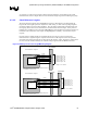
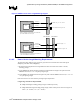
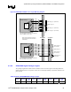
Figure 38. SDQ/SDM to SDQS Trace Length Matching Diagram
SO-DIMM0
GMCH Package
Note: All lengths are measured from GMCH die
pad to SO-DIMM connector pad.
SDQ[0]
SDQ[1]
SDQ[2]
SDQ[3]
SDQS[0]
SDQ[4]
SDQ[5]
SDQ[6]
SDQ[7]
SDQ Length (Y) = (X ±25 mils)
SDQ Length (Y) = (X ±25 mils)
SDQS Length = X
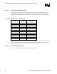
SO-DIMM0 SO-DIMM1
GMCH Package
SDQ[0]
SDQ[1]
SDQ[2]
SDQ[3]
SDQS[0]
SDQ[4]
SDQ[5]
SDQ[6]
SDQ[7]
SDQ Length (Y) =
(X +/-25 mils)
SDQ Length (Y) =
(X +/-25 mils)
SDQS Length = X
Note: All lengths are measured from GMCH die-
pad to SO-DIMM connector pads.
GMCH
Die
GMCH
Die
SDM[0]
SDM Length (Y) = (X ±25 mils)
SDM Length (Y) =
(X ±25 mils)
SDM[0]
Note: Only one byte lane is shown for
reference. Each byte lane is matched
independently.
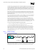
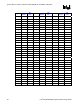
6.3.4.5. SDQ/SDQS Signal Package Lengths
The package length data in Table 28 below should be used to tune the length of each SDQ, SDM, and
SDQS motherboard trace as required to achieve the overall length matching requirements defined in the
prior Sections.
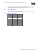
Table 28. Memory SDQ/SDM/SDQS Package Lengths
Signal
Pin
Number
Pkg
Length
(mils)
Signal
Pin
Number
Pkg
Length
(mils)
Signal
Pin
Number
Pkg
Length
(mils)
SDQ_00 AF2 785 SDQ_24 AH10 648 SDQ_48 AE23 592