
Design Guide

System Memory Design Guidelines (DDR-SDRAM) for SO-DIMM configuration
R
92 Intel
®
855GM/855GME Chipset Platform Design Guide
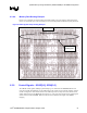
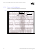
Table 29. Control Signal to SO-DIMM Mapping
Signal Relative To SO-DIMM Pin
SCS#[0] SO-DIMM0 AD23
SCS#[1] SO-DIMM0 AD26
SCS#[2] SO-DIMM1 AC22
SCS#[3] SO-DIMM1 AC25
SCKE[0] SO-DIMM0 AC7
SCKE[1] SO-DIMM0 AB7
SCKE[2] SO-DIMM1 AC9
SCKE[3] SO-DIMM1 AC10
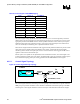
The control signal routing should transition from an external layer to an internal signal layer under the
GMCH, keep to the same internal layer until transitioning back out to an external layer to connect to the
appropriate pad of the SO-DIMM connector and the parallel termination resistor. If the layout requires
additional routing before the termination resistor, return to the same internal layer and transition back
out to an external layer immediately prior to parallel termination resistor.
External trace lengths should be minimized. Intel suggests that the parallel termination be placed on both
sides of the board to simplify routing and minimize trace lengths. All internal and external signals
should be ground reference to keep the path of return current continuous. Intel suggests that all control
signals be routed on the same internal layer.
Resistor packs are acceptable for the parallel (Rt) control termination resistors, but control signals can’t
be placed within the same R pack as the data or command signals. Figure 40 and Table 30 below depicts
the recommended topology and layout routing guidelines for the DDR-SDRAM control signals.
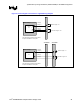
6.3.5.1. Control Signal Topology
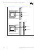
Figure 40. Control Signal Routing Topology
P1
Vtt
SO-DIMM0,1 PAD
w
Rt
L2
GMCH
Pin
GMCH
L1
S1
The control signals should be routed using 2 to 1 trace spacing to trace width ratio for signals within the
DDR group, except clocks and strobes. There should be a minimum of 20-mils of spacing to non-DDR
related signals. Control signals should be routed on inner layers with minimized external trace lengths.