
Design Guide

System Memory Design Guidelines (DDR-SDRAM) for SO-DIMM configuration
R
Intel
®
855GM/855GME Chipset Platform Design Guide 93
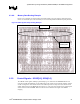
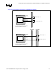
6.3.5.2. Control Signal Routing Guidelines
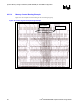
Table 30. Control Signal Routing Guidelines
Parameter Routing Guidelines
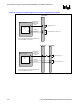
Signal Group SCKE[3:0], SCS#[3:0]
Motherboard Topology Point-to-Point with Parallel Termination
Reference Plane Ground Referenced
Characteristic Trace Impedance (Zo) 55 Ω ±15%
Nominal Trace Width
Inner layers: 4 mils
Outer layers: 5 mils
Minimum Spacing to Trace Width Ratio 2 to 1 (e.g. 8 mil space to 4 mil trace)
Minimum Isolation Spacing to non-DDR Signals 20 mils
Package Length P1 500 mils +/- 250 mils (Refer to Table 31 for details)
Stub Length S1 – Stub from Via to SO-DIMM Pad Max = 0.25”
Trace Length L1+S1 – Total length from GMCH Signal Ball to
SO-DIMM Pad
Min = 0.5 inches
Max = 5.5 inches for DDR 266
Max = 4.5 inches for DDR 333
Trace Length L2 – SO-DIMM via to Parallel Termination
Resistor Pad
Max = 2.0 inches
Parallel Termination Resistor (Rt) 56 Ω ± 5%
Maximum Recommended Motherboard Via Count Per Signal 3
Length Matching Requirements
CTRL to SCK/SCK# [5:0] See length matching
Section 6.3.5.3 and Figure 41.
NOTES:
1. Recommended resistor values and trace lengths may change in a later revision of the design guide.
2. Power distribution vias from Rt to Vtt are not included in this count.
3. It is possible to route using 2 vias if one via is shared that connects to the SO-DIMM pad and parallel
termination resistor.
4. The overall maximum and minimum length to the SO-DIMM must comply with clock length matching
requirements.