
Design Guide

System Memory Design Guidelines (DDR-SDRAM) for SO-DIMM configuration
R
Intel
®
855GM/855GME Chipset Platform Design Guide 97
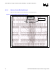
6.3.5.5. Control Group Package Length Table
The package length data in Table 31 below should be used to match the overall length of each command
signal to it’s associated clock reference length. Note that due to the relatively small variance in package
length and adequate timing margins it is acceptable to use a fixed 500-mil nominal package length for
all control signals, thereby reducing the complexity of the motherboard length calculations.
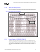
Table 31. Control Group Package Lengths
Signal Pin Number
Package
Length (mils)
Signal
Pin
Number
Package
Length (mils)
SCS#[0] AD23 502 SCKE[0] AC7 443
SCS#[1] AD26 659 SCKE[1] AB7 389
SCS#[2] AC22 544 SCKE[2] AC9 386
SCS#[3] AC25 612 SCKE[3] AC10 376
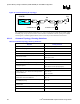
6.3.6. Command Signals – SMA[12:6,3,0], SBA[1:0], SRAS#, SCAS#,
SWE#
The GMCH chipset command signals, SMA[12:0], SBA[1:0], SRAS#, SCAS#, and SWE# clocked into
the DDR SDRAMs using the clock signals SCK/SCK#[5:0]. The GMCH drives the command and clock
signals together, with the clocks crossing in the valid command window. There are three supported
topologies for the command signal group. Topology 1 is a daisy chain topology. Topology 2 implements
a T routing topology. Both topologies allow series resistors to be placed between the two SO-DIMMs to
dampen the SO-DIMM to SO-DIMM resonance. Topology 2 is the topology that best allows for
placement of the SO-DIMMs back to back in the butterfly configuration, thus minimizing the SO-
DIMM footprint area. Topology 3 allows the series resistors to be physically placed after the farthest
SO-DIMM, when there is no room between the two connectors. Note that series resistors are essential in
all of the three topologies.
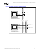
6.3.6.1. Command Topology 1
The command signal routing should transition from an external layer to an internal signal layer under
the GMCH. Keep to the same internal layer until transitioning back to an external layer immediately
prior to connecting the SO-DIMM0 connector pad. At the via transition for SO-DIMM0, continue the
signal route on the same internal layer to the series termination resistor (Rs), collocated to SO-DIMM1.
At this resistor the signal should transition to an external layer immediately prior to the pad of Rs. After
the series resistor, Rs, continue the signal route on the external layer landing on the appropriate
connector pad of SO-DIMM1. After SO-DIMM1, transition to the same internal layer or stay on the
external layer and route the signal to Rt.
Intel suggests that the parallel termination (Rt) be placed on both sides of the board to simplify routing
and minimize trace lengths. All internal and external signals should be ground referenced to keep the
path of the return current continuous.
Resistor packs are acceptable for the series and parallel command termination resistors but command
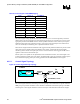
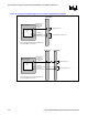
signals can’t be placed within the same R-packs as data, strobe, or control signals. Figure 43 and Table
32 below depict the recommended topology and layout routing guidelines for the DDR-SDRAM
command signals routing to SO-DIMM0 and SO-DIMM1.