
Design Guide

System Memory Design Guidelines (DDR-SDRAM) for SO-DIMM configuration
R
98 Intel
®
855GM/855GME Chipset Platform Design Guide
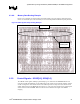
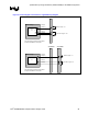
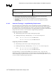
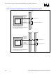
Figure 43. Command Routing for Topology 1
w
Rs
SO-DIMM1 PADSO-DIMM0 PAD
Vt
t
GMCH
P1
L3
w
L2
Rt
L4
GMCH
Pin
L1
S0
S1
The command signals should be routed using a 2 to 1 trace spacing to trace width ratio for signals within
the DDR group, except clocks and strobes. There should be a minimum of 20 mils spacing to non-DDR
related signals. Command signals should be routed on inner layers with minimized external traces.
6.3.6.2. Command Topology 1 Routing Guidelines
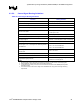
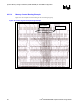
Table 32. Command Topology 1 Routing Guidelines
Parameter Routing Guidelines
Signal Group SMA[12:6,3,0], SBA[1:0], SRAS#, SCAS#, SWE#
Motherboard Topology Daisy Chain with Parallel Termination
Reference Plane Ground Referenced
Characteristic Trace Impedance (Zo) 55 Ω ± 15%
Nominal Trace Width
Inner layers: 4 mils
Outer layers: 5 mils
Minimum Spacing to Trace Width Ratio 2 to 1 (e.g. 8 mil space to 4 mil trace)
Minimum Isolation Spacing to non-DDR Signals 20 mils
Package Length P1
500 mils +/- 250 mils
(See Table 35 for exact package lengths.)
Stub Lengths S0, S1 Max = 0.25”
Trace Length L1 + S0 – GMCH Command Signal Ball to
First SO-DIMM Pad
Min = 0.5 inch
Max = 4.0 inches
Total Length L1 + L2 + L3 + S1 – Total Length from
GMCH Ball to Second SO-DIMM Pad
Min = 1.0”
Max = 7.0”
Total Length S0 + L2 + L3 + S1– Total SO-DIMM pad to
SO-DIMM pad spacing
Max = 3.0”
Trace Length L4 – Second SO-DIMM Via to Parallel
Resistor Pad
Max = 1.5 inches
Series Termination Resistor (Rs) 10 Ω ± 5%
Parallel Termination Resistor (Rt) 56 Ω ± 5%