
Document


Electrical Specifications
26 Datasheet
NOTES:
1. Unless otherwise noted, all specifications in this table apply to all processor frequencies.
2. Crossing Voltage is defined as absolute voltage where rising edge of BCLK0 is equal to the
falling edge of BCLK1.
3. For Vin between 0 V and V
IH
.
4. Cpad includes die capacitance only. No package parasitics are included.
5. ΔV
CROSS
is defined as the total variation of all crossing voltages as defined in Note 2.
6. Measurement taken from differential waveform.
7. Measurement taken from single-ended waveform.
8. Only applies to the differential rising edge (Clock rising and Clock# falling).
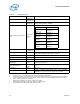
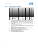
Table 7. FSB Differential BCLK Specifications
Symbol Parameter Min Typ Max Unit Notes
1
V
CROSS
Crossing Voltage 0.3 0.55 V 2, 7, 8
ΔV
CROSS
Range of Crossing Points 140 mV 2, 7, 5
V
SWING
Differential Output Swing 300 mV 6
I
LI
Input Leakage Current -5 +5 µA 3
Cpad Pad Capacitance 0.95 1.2 1.45 pF 4