
Intel Celeron Processor for the PGA370 Socket up to 1.40 GHz on 0.13 Micron Process Datasheet

Datasheet 29
Intel
®
Celeron
®
Processor for PGA370 up to 1.40 GHz on 0.13 µ Process
NOTES:
1. Unless otherwise noted, all specifications in this table apply to the processor at a frequency up to 1.40 GHz
on 0.13 micron.
2. All inputs, outputs, and I/O pins must comply with the signal quality specifications in Section 3.0.
3. Minimum and maximum V
TT are given in Table 13 on page 30.
4. (0
≤ VIN ≤ 1.25 V +3%) and (0≤VOUT≤1.25 V+3%).
5. Refer to the processor I/O Buffer Models for I/V characteristics.
6. Steady state input voltage must not be above V
SS + 1.65 V or below VTT – 1.65 V.
7. Does not apply to Vcc leakage current due to the presence of on-die RTT.
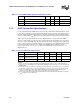
NOTES:
1. Unless otherwise noted, all specifications in this table apply to the processor up to 1.40 GHz frequency on
0.13 micron.
2. Parameter measured at 9 mA (for use with TTL inputs).
3. (0
≤ VIN ≤ 1.8 V +10%).
4. (0
≤ VOUT ≤ 1.8 V +10%).
5. For BCLK specifications, refer to Table 24 on page 41.
6. (0
≤ VIN ≤ 1.5 V +10%).
7. (0
≤ VOUT ≤ 1.5 V +10%).
8. Applies to non-AGTL signal PWRGOOD.
9. Applies to non-AGTL signal PICCLK.
10.Applies to non-AGTL signals
except BCLK, PICCLK, and PWRGOOD.
11.Applies to non-AGTL signal VTT_PWRGD.
12.Vcmos_ref = 2/3 Vcc_cmos1.5, refer to Table 7 on page 26.
13.Applies to PICD[1:0] only
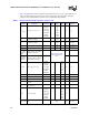
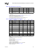
Table 10. AGTL Signal Group Levels Specifications
Symbol Parameter Min Max Unit Notes
1
VIL Input Low Voltage V
REF
- 0.200 V 6
V
IH Input High Voltage V
REF
+ 0.200 V 2, 3, 6
Ron Buffer On Resistance 16.67
Ω 5
I
L
Leakage Current for inputs,
outputs, and I/O
±100 µA 4, 7
Table 11. Non-AGTL Signal Group Levels Specifications
Symbol Parameter Min Max Unit Notes
1
VIL
1.2
Input Low Voltage 0.4 V 11
V
IL
1.5
Input Low Voltage –0.150 Vcmos_ref - 0.300 V 10
V
IL
1.8
Input Low Voltage -0.36 0.36 V 8
V
IL
2.0
Input Low Voltage -0.40 0.40 V 9
V
IH
1.2
Input High Voltage 1.03 V 11
V
IH
1.5
Input High Voltage
Vcmos_ref +
0.250
V
CC_CMOS1.5 +
10%
V 6, 10, 12
V
IH
1.5PICD
Input High Voltage PICD[1:0]
Vcmos_ref +
0.200
2.0 V 12, 13
V
IH
1.8
Input High Voltage 1.44 2.16 V 8
V
IH
2.0
Input High Voltage 1.60 V 9
R
on
30 Ω 2
V
OL Output Low Voltage 0.30 V
7, 9, All
outputs are
open-drain
I
OL Output Low Current 10 mA
I
LI Input Leakage Current ±100 µA 3, 6
I
LO Output Leakage Current ±100 µA 3, 4, 6, 7