
Intel Celeron Processor for the PGA370 Socket up to 1.40 GHz on 0.13 Micron Process Datasheet

32 Datasheet
Intel
®
Celeron
®
Processor for PGA370 up to 1.40 GHz on 0.13 µ Process
1. Unless otherwise noted, all specifications in this table apply to the processor up to 1.40 GHz frequency on
0.13 micron process.
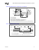
2. All timings for the AGTL signals are referenced at the rising edge of BCLK and the falling edge of BCLK# at
the processor pin. All AGTL signal timings (address bus, data bus, etc.) are referenced at 1.00 V at the
processor pins.
3. The internal core clock frequency is derived from the processor system bus clock. The system bus clock to
core clock ratio is determined during initialization. Individual processors will only operate at their specified
system bus frequency, 100 MHz. Table 16 shows the supported ratios for each processor.
4. Due to the difficulty of accurately measuring clock jitter in a system, it is recommended that a clock driver be
used that is designed to meet the period stability specification into a test load of 10 to 20 pF. This should be
measured at adjacent crossing points of BCLK and BCLK# which is defined as the rising edge of BCLK and
the falling edge of BCLK#
at the processor pin. The jitter present must be accounted for as a component of
BCLK timing skew between devices.
5. The clock driver’s closed loop jitter bandwidth must be set low to allow any PLL-based device to track the
jitter created by the clock driver. The –20 dB attenuation point, as measured into a 10 to 20 pF load, should
be less than
500 kHz. This specification may be ensured by design characterization and/or measured with a
spectrum analyzer. See the appropriate clock synthesizer/driver specification for details
6. Measurement taken from differential waveform, defined as BCLK – BCLK#.
7. Rise time is measured from -0.35 to +0.35V and fall time is measured from 0.35 V to -0.35 V.
8. Measured at the socket pin.
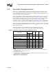
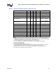
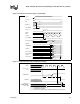
Table 15. System Bus Timing Specifications (Differential Clock)
T# Parameter
100 MHz
Unit Figure Notes
1,2,6
Min Max
T1: BCLK Period - average 10.0 10.2 nS 9 3, 4
T1
abs
: BCLK Period - Instantaneous minimum 9.8 nS 3, 4
T2: BCLK Period Stability 200 pS 5
Vcross: Crossing point at 1V Swing 0.51 0.76 V 9
T5: BCLK Rise Time 175 550 pS 10 7, 8
T6: BCLK Fall Time 175 550 pS 10 7, 8
Rise/Fall Time Matching 325 pS
BCLK Duty Cycle 45% 55% 4
Input High Voltage 0.92 1.45 V
Input Low Voltage -0.2 0.35 V
Rising Edge Ring Back 0.35 V
Falling Edge Ring Back -0.35 V