
Intel Celeron Processor for the PGA370 Socket up to 1.40 GHz on 0.13 Micron Process Datasheet

Datasheet 33
Intel
®
Celeron
®
Processor for PGA370 up to 1.40 GHz on 0.13 µ Process
NOTES:
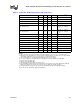
1. Contact your local Intel representative for the latest information on processor frequencies and/or frequency
multipliers.
2. While other bus ratios are defined, operation at frequencies other than those listed are not supported by the
processor.
3. Individual processors will only operate at their specified system bus frequency; 100 MHz.
4. 1.20 GHz at Vcc
CORE
= 1.475 volts and S-Spec number SL5XS.
NOTES:
1. Unless otherwise noted, all specifications in this table apply to the processor up to 1.40 GHz on 0.13 micron
process.
2. These specifications are tested during manufacturing.
3. All timings for the AGTL signals are referenced to the rising edge of BCLK and the falling edge of BCLK# at
the processor pin. All AGTL signal timings (compatibility signals, etc.) are referenced at 0.80 V at the
processor pins.
4. Valid delay timings for these signals are specified into 50
Ω to 1.25 V, V
REF
at 0.8 V ±2% and with 56 Ω or
68
Ω on-die R
TT
.
5. A minimum of 3 clocks must be guaranteed between two active-to-inactive transitions of TRDY#.
6. RESET# can be asserted (active) asynchronously, but must be deasserted synchronously.
7. Specification is for a minimum 0.40 V swing from V
REF
– 200 mV to V
REF
+ 200 mV. This assumes an edge
rate of 0.3V/ns.
8. Specification is for a maximum 0.8 V swing from V
TT – 0.8V to VTT. This assumes an edge rate of 3 V/ns.
9. This should be measured after V
CC
CORE
, VTT, Vcc
CMOS
, and BCLK (and BCLK#) are stable
10.BREQ signals observe a 1.2 ns minimum setup time.
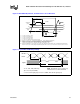
NOTES:
1. Unless otherwise noted, all specifications in this table apply to the processor up to 1.40 GHz frequency
2. These specifications are tested during manufacturing.
3. These signals may be driven asynchronously.
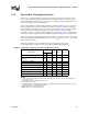
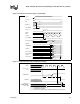
Table 16. Valid System Bus to Core Frequency Ratios
1, 2, 3
Processor Core Frequency
BCLK Frequency
(MHz)
Frequency
Multiplier
1.4 GHz 1.40 100 14
1.30 1.30 GHz 100 13
1.20 1.20 GHz 100 12
1.20
4
1.20
4
GHz 100 12
1.1A 1.1A GHz 100 11
1A 1A GHz 100 10
900 900 MHz 100 9
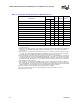
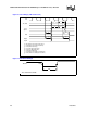
Table 17. System Bus Timing Specifications (AGTL Signal Group)
T# Parameter Min Max Unit Figure Notes
1,2,3
T7: AGTL Output Valid Delay 0.40 3.25 ns 11 4
T8: AGTL Input Setup Time 1.30 ns 12 5, 6, 7, 10
T9: AGTL Input Hold Time 1.00 ns 12 8
T10: RESET# Pulse Width 1.00 ms 13 6, 9
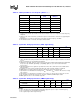
Table 18. System Bus Timing Specifications (CMOS Signal Group)
T# Parameter Min Max Unit Figure Notes 1
,2,3,4
T14: CMOS Input Pulse Width, except
PWRGOOD
2 BCLKs 11
Active and
Inactive states
T15: PWRGOOD Inactive Pulse Width 10 BCLKs 15 5