
Intel Celeron Processor for the PGA370 Socket up to 1.40 GHz on 0.13 Micron Process Datasheet

34 Datasheet
Intel
®
Celeron
®
Processor for PGA370 up to 1.40 GHz on 0.13 µ Process
4. All CMOS outputs shall be asserted for at least 2 system bus clocks.
5. When driven inactive or after V
CC
CORE
, VTT, VCC
CMOS
, and BCLK and BCLK# are stable.
NOTE:
1. Unless otherwise noted, all specifications in this table apply to all the processor up to 1.40 GHz frequency.
NOTES:
1. Unless otherwise noted, all specifications in this table apply to the processor up to 1.40 GHz frequency.
2. These specifications are tested during manufacturing.
3. All timings for the APIC I/O signals are referenced to the PICCLK rising edge at 0.9 V at the processor pins.
All APIC I/O signal timings are referenced at 1.0 V at the processor pins.
4. Referenced to PICCLK rising edge.
5. For open drain signals, valid delay is synonymous with float delay.
6. Valid delay timings for these signals are specified into 150
Ω load pulled up to 1.5 V.
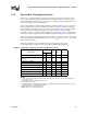
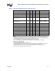
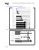
Table 19. System Bus Timing Specifications (Reset Conditions)
1
T# Parameter Min Max Unit Figure Notes
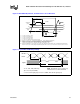
T16: Reset Configuration Signals
(A[14:5]#, BR0#, INIT#) Setup Time
4 BCLKs 13
Before deassertion
of RESET#
T17: Reset Configuration Signals
(A[14:5]#, BR0#, INIT#) Hold Time
2 20 BCLKs 13
After clock that
deasserts RESET#
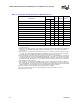
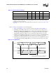
Table 20. System Bus Timing Specifications (APIC Clock and APIC I/O)
1, 2, 3
T# Parameter Min Max Unit Figure Notes
T21: PICCLK Frequency 2.0 33.3 MHz
T22: PICCLK Period 30.0 500.0 ns 10
T23: PICCLK High Time 10.5 ns 10 @ > 1.60 V
T24: PICCLK Low Time 10.5 ns 10 @ < 0.40 V
T25: PICCLK Rise Time 0.25 3.0 ns 10 (0.40 V – 1.60 V)
T26: PICCLK Fall Time 0.25 3.0 ns 10 (1.60 – 0.40 V)
T27: PICD[1:0] Setup Time 8.0 ns 12 4
T28: PICD[1:0] Hold Time 2.5 ns 12 4
T29a: PICD[1:0] Valid Delay (Rising Edge) 1.5 8.7 ns 11 4, 5, 6
T29b: PICD[1:0] Valid Delay (Falling Edge) 1.5 12.0 ns 10 4, 5, 6