
Intel Celeron Processor for the PGA370 Socket up to 1.40 GHz on 0.13 Micron Process Datasheet

Datasheet 35
Intel
®
Celeron
®
Processor for PGA370 up to 1.40 GHz on 0.13 µ Process
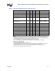
NOTES:
1. Unless otherwise noted, all specifications in this table apply to the processor up to 1.40 GHz frequency.
2. All timings for the TAP signals are referenced to the TCK rising edge at 1.0 V at the processor pins. All TAP
signal timings (TMS, TDI, etc.) are referenced at 1.0 V at the processor pins.
3. These specifications are tested during manufacturing, unless otherwise noted.
4. 1 ns can be added to the maximum TCK rise and fall times for every 1 MHz below 16.667 MHz.
5. Referenced to TCK rising edge.
6. Referenced to TCK falling edge.
7. Valid delay timing for this signal is specified to 1.5 V.
8. Non-Test Outputs and Inputs are the normal output or input signals (besides TCK, TRST#, TDI, TDO, and
TMS). These timings correspond to the response of these signals due to TAP operations.
9. During Debug Port operation, use the normal specified timings rather than the TAP signal timings.
10.Not 100% tested. Specified by design characterization.
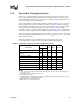
Table 21. System Bus Timing Specifications (TAP Connection)
T# Parameter Min Max Unit Figure Notes
1,2,3
T30: TCK Frequency 16.667 MHz
T31: TCK Period 60.0 ns 10
T32: TCK High Time 25.0 ns 10 Vcmos_ref + 0.200 V, 10
T33: TCK Low Time 25.0 ns 10 Vcmos_ref – 0.200 V, 10
T34: TCK Rise Time 5.0 ns 10
(Vcmos_ref – 0.200 V) –
(Vcmos_ref + 0.200 V),
4, 10
T35: TCK Fall Time 5.0 ns 10
(Vcmos_ref + 0.200 V) –
(Vcmos_ref – 0.200 V),
4, 10
T36: TRST# Pulse Width 40.0 ns 17 Asynchronous, 10
T37: TDI, TMS Setup Time 5.0 ns 16 5
T38: TDI, TMS Hold Time 14.0 ns 16 5
T39: TDO Valid Delay 1.0 10.0 ns 16 6, 7
T40: TDO Float Delay 25.0 ns 16 6, 7, 10
T41: All Non-Test Outputs Valid Delay 2.0 25.0 ns 16 6, 8, 9
T42: All Non-Test Inputs Setup Time 25.0 ns 16 6, 8, 9, 10
T43: All Non-Test Inputs Setup Time 5.0 ns 16 5, 8, 9
T44: All Non-Test Inputs Hold Time 13.0 ns 16 5, 8, 9